21098765432121098765432109876543210987654321210987654321098765432109876543212109876543210987654321098765432121098765432109876543210987654321
21098765432121098765432109876543210987654321210987654321098765432109876543212109876543210987654321098765432121098765432109876543210987654321
錚?/div>
Description
Features
鈥?PI6C3Q99X family provides following products:
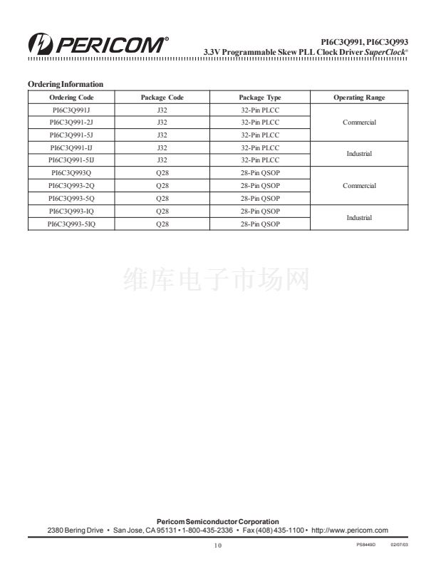
PI6C3Q991: 32-pin PLCC version
PI6C3Q993: 28-pin QSOP version
鈥?Inputs are 5V Tolerant
鈥?4 pairs of programmable skew outputs
鈥?Low skew: 200ps same pair; 250ps all outputs
鈥?Selectable positive or negative edge synchronization:
Excellent for DSP applications
鈥?Synchronous output enable
鈥?Input frequency: 3.75 MHz to 85 MHz
鈥?Output frequency: 15 MHz to 85MHz
鈥?2x, 4x, 1/2, and 1/4 outputs
鈥?3 skew grades:
PI6C3Q99x: t
SKEW0
<750ps
PI6C3Q99x-5: t
SKEW0
<500ps
PI6C3Q99x-2: t
SKEW0
<250ps
鈥?3-level inputs for skew and PLL range control
鈥?PLL bypass for DC testing
鈥?External feedback, internal loop filter
鈥?12mA balanced drive outputs
鈥?Low Jitter: < 200ps peak-to-peak
鈥?Industrial temperature range
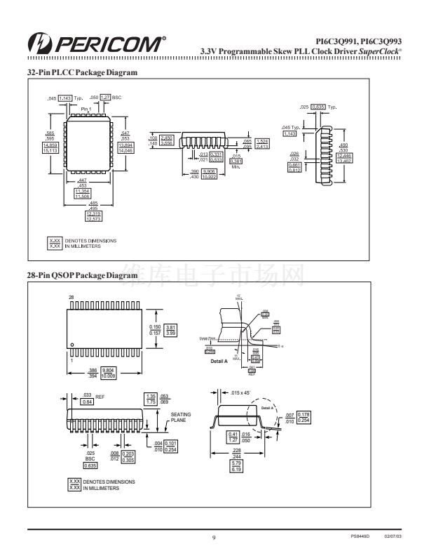
鈥?Available in 32-pin PLCC and 28-pin QSOP
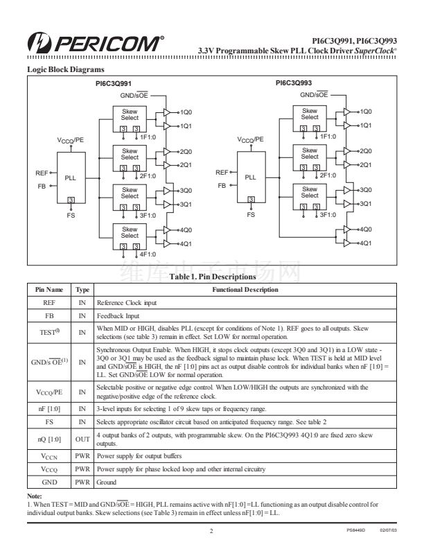
The PI6C3Q99X family, a high-fanout 3.3V PLL-based clock driver,
is intended for high-performance computing and data-communica-
tion applications. A key feature of the programmable skew is the
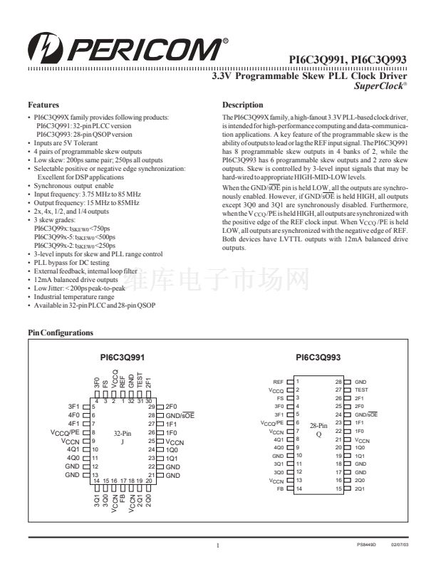
ability of outputs to lead or lag the REF input signal. The PI6C3Q991
has 8 programmable skew outputs in 4 banks of 2, while the
PI6C3Q993 has 6 programmable skew outputs and 2 zero skew
outputs. Skew is controlled by 3-level input signals that may be
hard-wired to appropriate HIGH-MID-LOW levels.
When the GND/sOE pin is held LOW, all the outputs are synchro-
nously enabled. However, if GND/sOE is held HIGH, all outputs
except 3Q0 and 3Q1 are synchronously disabled. Furthermore,
when the V
CCQ
/PE is held HIGH, all outputs are synchronized with
the positive edge of the REF clock input. When V
CCQ
/PE is held
LOW, all outputs are synchronized with the negative edge of REF.
Both devices have LVTTL outputs with 12mA balanced drive
outputs.
Pin Configurations
PI6C3Q991
REF
VCCQ
FS
PI6C3Q993
1
2
3
4
5
6
7
8
9
10
11
12
13
14
28
27
26
25
24
23
22
21
20
19
18
17
16
15
GND
TEST
2F1
2F0
GND/sOE
1F1
1F0
VCCN
1Q0
1Q1
GND
GND
2Q0
2Q1
3F1
4F0
4F1
VCCQ/PE
VCCN
4Q1
4Q0
GND
GND
4
5
6
7
8
9
10
11
12
3 2
1 32 31 30
29
28
27
26
32-Pin
25
J
24
23
22
13
21
14 15 16 17 18 19 20
2F0
GND/sOE
1F1
1F0
VCCN
1Q0
1Q1
GND
GND
3F0
3F1
VCCQ/PE
VCCN
4Q1
4Q0
GND
3Q1
3Q0
VCCN
FB
28-Pin
Q
1
PS8449D
02/07/03


 1
1
 2
2
 3
3
 4
4
 5
5
 6
6
 7
7
 8
8
 9
9
 10
10
