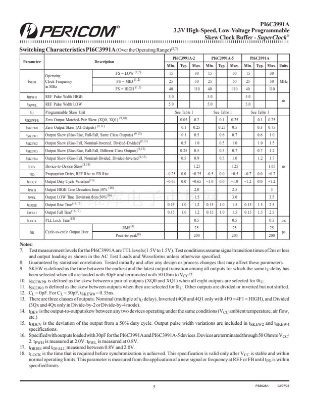
Freq.
21098765432121098765432109876543210987654321210987654321098765432109876543212109876543210987654321098765432121098765432109876543210987654321
21098765432121098765432109876543210987654321210987654321098765432109876543212109876543210987654321098765432121098765432109876543210987654321
錚?/div>
Features
鈥?All output pair skew <100ps typical (250 Max.)
鈥?3.75 MHz to 110 MHz output operation
鈥?User-selectable output functions
鈥?Selectable skew to 18ns
鈥?Inverted and Non-Inverted
鈥?Operation at 錕?frac12; and 錄 input frequency
鈥?Operation at 2X and 4X input frequency
(input as low as 3.75 MHz, x4 operation)
鈥?Zero input-to-output delay
鈥?50% duty-cycle outputs
鈥?Inputs are 5V Tolerant
鈥?LVTTL outputs drive 50-ohm terminated lines
鈥?Operates from a single 3.3V supply
鈥?Low operating current
鈥?Available in 32-pin PLCC (J) package
鈥?Jitter < 200ps peak-to-peak (< 25ps RMS)
鈥?Pin-to-Pin compatible with CY7B991V
Description
PI6C3991A offers selectable control over system clock functions.
These multiple-output clock drivers provide the system integrator
with functions necessary to optimize the timing of high-perfor-
mance computer systems. Eight individual drivers, arranged as four
pairs of user-controllable outputs, can each drive terminated trans-
mission lines with impedances as low as 50-ohms while delivering
minimal and specified output skews and full-swing logic levels
(LVTTL).
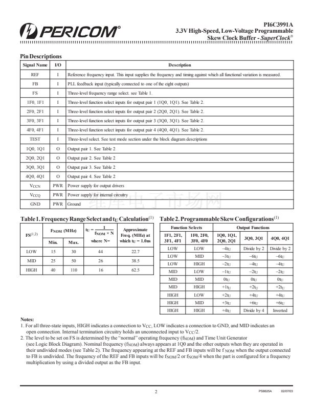
Each output can be hardwired to one of nine skews or function
configurations. Delay increments of 0.7ns to 1.5ns are determined
by the operating frequency with outputs able to skew up to 鹵6 time
units from their nominal 鈥渮ero鈥?skew position. The completely
integrated PLL allows external load and transmission line delay
effects to be canceled. The user can create output-to-output skew
up to 鹵12 time units.
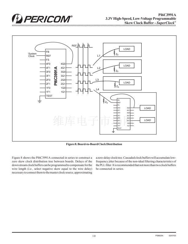
Divide-by-two and divide-by-four output functions are provided
for additional flexibility in designing complex clock systems. When
combined with the internal PLL, these divide functions allow
distribution of a low-frequency clock that can be multiplied by
two or four at the clock destination. This feature allows flexibility
and simplifies system timing distribution design for complex
high-speed systems.
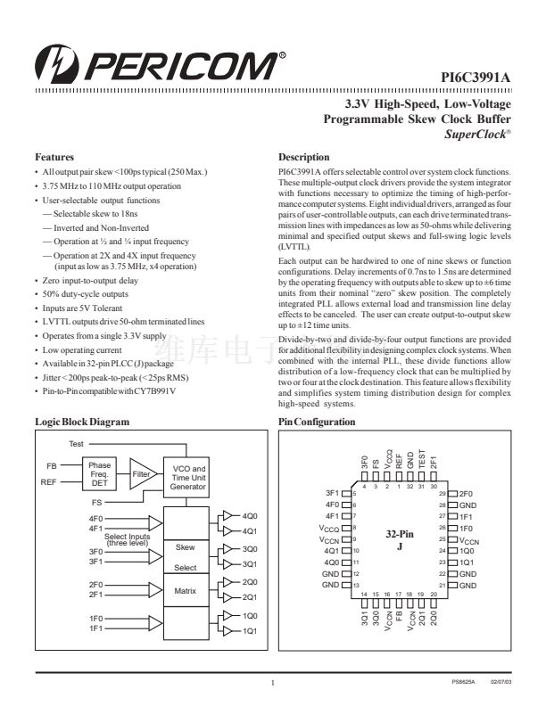
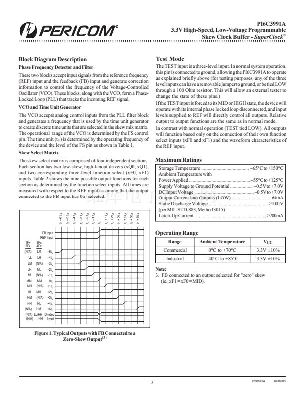
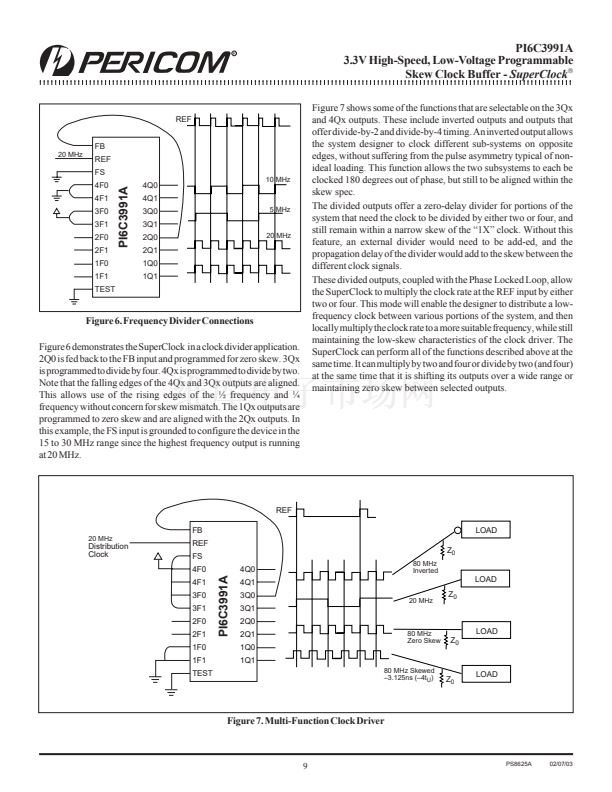
Logic Block Diagram
Test
Pin Configuration
5
6
7
8
9
10
11
12
13
14 15 16 17 18 19
20
3F0
3F1
2F0
2F1
32-Pin
J
26
25
24
23
22
21
2F0
GND
1F1
1F0
V
CCN
1Q0
1Q1
GND
GND
1
PS8625A
02/07/03


 1
1
 2
2
 3
3
 4
4
 5
5
 6
6
 7
7
 8
8
 9
9
 10
10
 11
11
