GNDO
VCCO
Qb2
Qb3
GNDO
GNDO
Qc0
Qc1
VCCO
24 23 22 21 20 19 18 17
16
25
15
26
27
28
29
30
31
32 1
2 3 4
5
6 7 8
GNDO
VCCO
VCCO
Qb1
Qb0
Qa4
Qa3
VCO_Sel
MR/OE
REFCLK
GNDI
fselc
fselb
fsela
FBin
21098765432121098765432109876543210987654321210987654321098765432109876543212109876543210987654321098765432121098765432109876543210987654321
21098765432121098765432109876543210987654321210987654321098765432109876543212109876543210987654321098765432121098765432109876543210987654321
21098765432121098765432109876543210987654321210987654321098765432109876543212109876543210987654321098765432121098765432109876543210987654321
PI6C2952
Low Voltage PLL Clock Driver
Features
聲 鹵100ps Cycle-to-Cycle Jitter
聲 Fully Integrated PLL
聲 Output Frequency up to 180MHz
聲 High-Impedance Disabled Outputs
聲 Compatible with PowerPC, Intel and High Performance
RISC Microprocessors
聲 Configurable Output Frequency
聲 32-Pin LQFP Package (FB)
Description
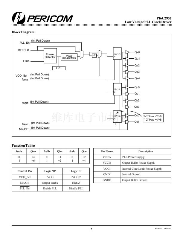
The PI6C2952 is a 3.3V compatible, PLL-based clock driver device
targeted for high-performance clock applications. The device fea-
tures a fully integrated PLL with no external components
required. With output frequencies up to 180MHz and eleven low-
skew outputs, the PI6C2952 is well suited for high-performance
designs. The device employs a fully differential PLL design to
optimize jitter and noise rejection performance.
The PI6C2952 features three banks of individually configurable
outputs. The banks contain 5 outputs, 4 outputs, and 2 outputs. The
internal divide circuitry allows for output frequency ratios of 1:1, 2:1,
3:1, and 3:2:1. The output frequency relationship is controlled by the
fsel frequency control pins. The fsel pins and other inputs are
LVCMOS/LVTTL compatible inputs.
The PI6C2952 uses external feedback to the PLL. This features allows
the device to be used as a 聯(lián)zero delay聰 buffer. Any of the eleven
outputs can be used as feedback to the PLL. To optimize PLL stability
and jitter performance,the VCO_Sel pin allows for the choice of two
VCO ranges. For board level test, the MR/OE pin allows a user to
force the outputs into high impedance. For system debug, the
PI6C2952聮s PLL can be bypassed. When forced to a logic HIGH, the
PLLEN input routes the signal on the RefClk input around the PLL
directly to the internal dividers. Because the signal is routed through
the dividers, it may take several transitions of the RefClk to affect a
transition on the outputs. This features allows a designer to single
step the design for debug purposes.
The PI6C2952聮s outputs are LVCMOS which are optimally designed
to drive terminated transmission lines. For applications using series-
terminated transmission lines, each PI6C2952 output can drive two
lines. This capability provides an effective fanout of 22, more than
enough clocks for most clock tree designs.
Pin Configuration
VCCO
Qa2
Qa1
GNDO
Qa0
VCCI
VCCA
PLL_En
32-Pin
FB
14
13
12
11
10
9
1
PS8542
06/20/01


 1
1
 2
2
 3
3
 4
4
 5
5
 6
6
