鈥?/div>
Space-saving Packages:
150-mil SOIC (W)
173-mil TSSOP (L)
Functional Description
The PI6C2409 is a PLL based, zero-delay buffer, with the ability
to distribute nine outputs of up to 133MHz at 3.3V.
All the outputs are distributed from a single clock input CLKIN and
output OUT0 performs zero delay by connecting a feedback to PLL.
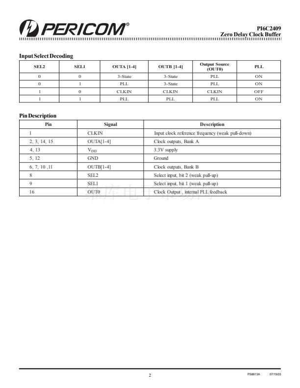
PI6C2409 has two banks of four outputs that can be controlled by
the selection inputs, SEL1 & SEL2. It also has a powersparing feature:
when input SEL1 is 0 and SEL2 is 1, PLL is turned off and all
outputs are referenced from CLKIN. PI6C2409 is available in
high drive and industrial environment versions.
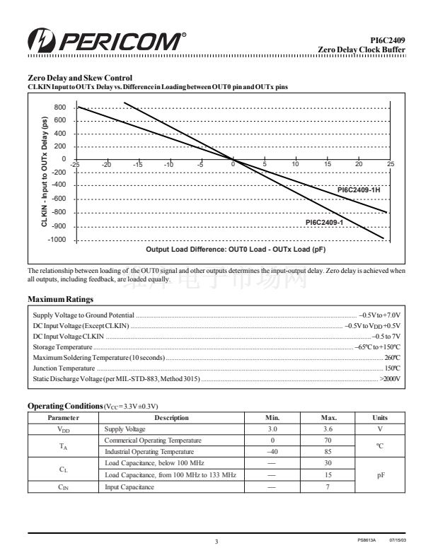
An internal feedback on OUT0 is used to synchronize the
outputs to the input; the relationship between loading of this signal
and the outputs determines the input-output delay.
PI6C2409 are characterized for both commercial and
industrial operation
Block Diagram
OUT0
CLKIN
PLL
MUX
OUTA1
OUTA2
OUTA3
SEL1
SEL2
Decode
Logic
OUTA4
OUTB1
OUTB2
PI6C2409(-1, -1H)
OUTB3
OUTB4
Pin Configuration
CLKIN
OUTA1
OUTA2
VDD
GND
OUTB1
OUTB2
SEL2
1
2
3
4
5
6
7
8
16
15
16-Pin
14
W, L
13
12
11
10
9
OUT0
OUTA4
OUTA3
VDD
GND
OUTB4
OUTB3
SEL1
1
PS8613A
07/15/03


 1
1
 2
2
 3
3
 4
4
 5
5
 6
6
 7
7
 8
8
