鈥?/div>
Maximum rated frequency: 133 MHz
Low cycle-to-cycle jitter
Input to output delay, less than 200ps
External feedback pin allows outputs to be synchronized
to the clock input
5V tolerant input*
Operates at 3.3V V
DD
Test mode allows bypass of the PLL for system testing
purposes (e.g., IBIS measurements)
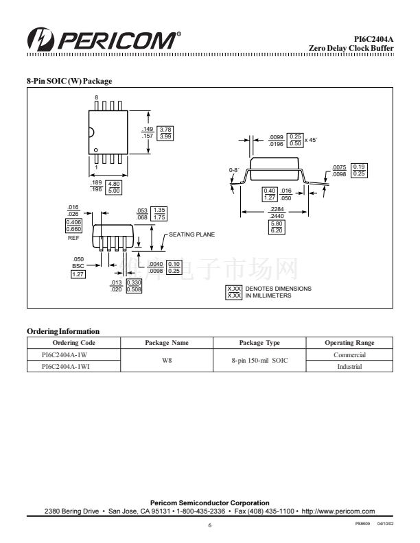
Space-saving Packages:
8-pin, 150-mil SOIC (W)
Functional Description
The PI6C2404A is a PLL-based, zero-delay buffer, with the ability
to distribute four outputs of up to 133 MHz at 3.3 V. Two banks of
two outputs exist, OUTA[1聳2) and OUTB[1聳2].
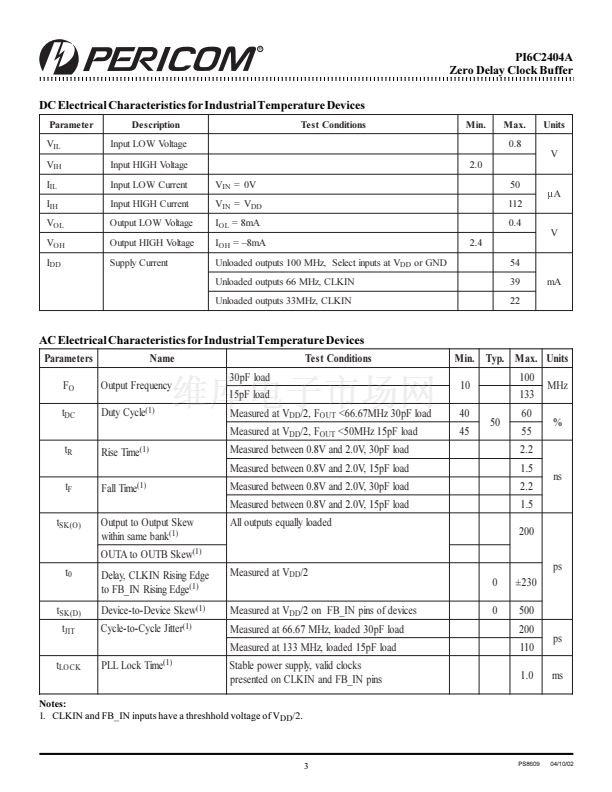
An external feedback pin is used to synchronize the outputs to the
input; the relationship between loading of this signal and the other
outputs determines the input-output delay.
The PI6C2404A is characterized for both commercial and industrial
operation.
* FB_IN and CLKIN must reference the same voltage thresh-
olds for the PLL to deliver zero delay skewing
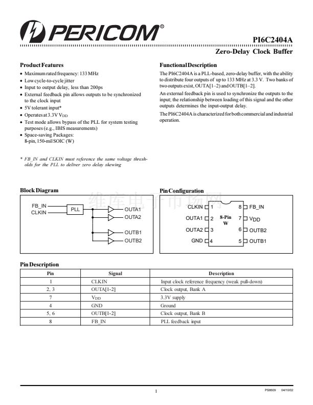
Block Diagram
FB_IN
CLKIN
PLL
OUTA1
OUTA2
OUTB1
OUTB2
Pin Configuration
CLKIN
OUTA1
OUTA2
GND
1
2
3
4
8-Pin
W
8
7
6
5
FB_IN
VDD
OUTB2
OUTB1
Pin Description
Pin
1
2, 3
7
4
5, 6
8
C LK IN
O UTA[1- 2]
V
DD
GN D
O UTB[1- 2]
FB_IN
Signal
C lock output, Bank A
3.3V supply
Ground
C lock output, Bank B
PLL feedback input
D e s cription
Input clock reference frequency (weak pull- down)
1
PS8609
04/10/02


 1
1
 2
2
 3
3
 4
4
 5
5
 6
6
