鈥?/div>
Available in industrial and commercial temperatures
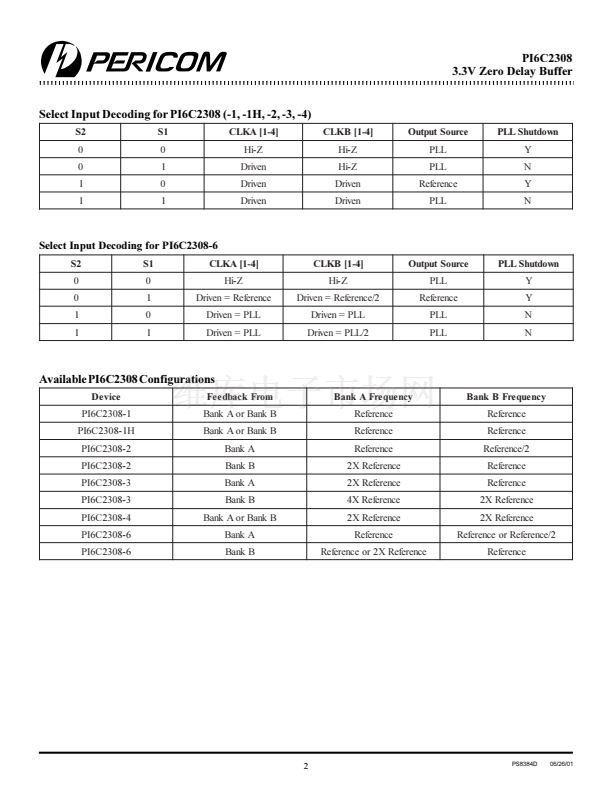
Functional Description
Providing two banks of four outputs, the PI6C2308 is a 3.3V zero-
delay buffer designed to distribute clock signals in applications
including PC, workstation, datacom, telecom, and high-performance
systems. Each bank of four outputs can be controlled by the select
inputs as shown in the Select Input Decoding Table.
The PI6C2308 provides 8 copies of a clock signal that has 200ps
phase error compared to a reference clock. The skew between the
output clock signals for PI6C2308 is less than 200ps. When there
are no rising edges on the REF input, the PI6C2308 enters a power
down state. In this mode, the PLL is off and all outputs are Hi-Z.
This results in less than 12碌A of current draw. The Select Input
Decoding Table shows additional examples when the PLL shuts
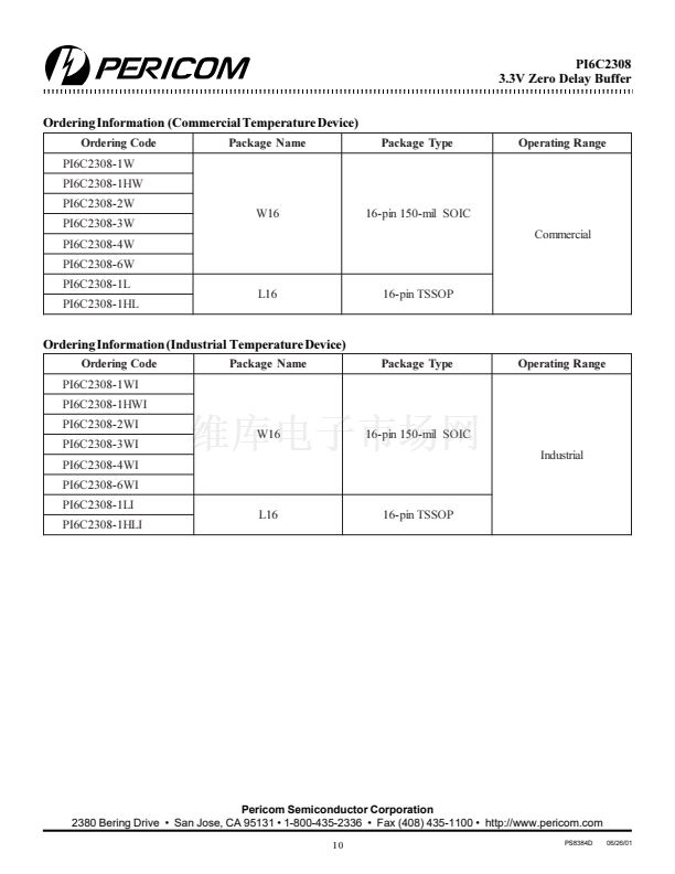
down. The PI6C2308 configuration table shows all available devices.
The base part, PI6C2308-1, provides output clocks in sync with a
reference clock. With faster rise and fall times, the PI6C2308-1H
is the high drive version of the PI6C2308-1. Depending on which
output drives the feedback pin, PI6C2308-2 provides 2X and 1X
clock signals on each output bank. The PI6C2308-3 allows the user
to obtain 4X and 2X frequencies on the outputs. The PI6C2308-4
provides 2X clock signals on all outputs. PI6C2308 (-1, -2, -3, -4) allows
bank B to be Hi-Z when all output clocks are not required.The
PI6C2308-6 allows bank B to switch from Reference clock to half
of the frequency of Reference clock using the control inputs S1 and
S2 if Bank A is connected to feedback FBK. In addition, using the
control inputs S1 and S2, the PI6C2308-6 allows bank A to switch
from Reference clock to 2X the frequency of Reference clock if
Bank B is connected to feedback FBK. For testing purposes, the
select inputs connect the input clock directly to outputs.
Block Diagrams
梅2
REF
PLL
MUX
FBK
CLKA1
CLKA2
Extra Divider (-3, -4)
CLKA3
CLKA4
梅2
CLKB1
S2
S1
Select Input
Decoding
Extra Divider (-2,-3)
CLKB2
CLKB3
PI6C2308 (-1, -1H, -2, -3, -4)
CLKB4
REF
PLL
MUX
S2
S1
Select Input
Decoding
梅2
MUX
FBK
CLKA1
CLKA2
CLKA3
CLKA4
Pin Configuration PI6C2308 (聳1, 聳1H, 聳2, 聳3, 聳4, 聳6)
REF
CLKA1
CLKA2
V
DD
GND
CLKB1
CLKB2
S2
1
2
3
4
5
6
7
8
16
15
14
16-Pin
13
W, L
12
11
10
9
FBK
CLKA4
CLKA3
V
DD
GND
CLKB4
CLKB3
S1
PI6C2308-6
CLKB1
CLKB2
CLKB3
CLKB4
1
PS8384D
06/26/01


 1
1
 2
2
 3
3
 4
4
 5
5
 6
6
 7
7
 8
8
 9
9
 10
10
