21098765432121098765432109876543210987654321210987654321098765432109876543212109876543210987654321098765432121098765432109876543210987654321
1
2109876543212109876543210987654321098765432121098765432109876543210987654321210987654321098765432109876543212109876543210987654321098765432
21098765432121098765432109876543210987654321210987654321098765432109876543212109876543210987654321098765432121098765432109876543210987654321
PI6C102-16
Spread Spectrum Clock Synthesizer
for Mobile Pentium II
Features
路 100 MHz or 66.6 MHz operation
路 Two copies of CPU clock with V
DD
of 2.5V
路 High drive option to support modular mobile CPUs
路 Six copies of PCI clock, (synchronous with CPU clock) 3.3V
路 One copy of Ref. Clock @ 14.31818 MHz (3.3V
TTL
)
路 One copy of 48 MHz Clock (3.3V)
路 Low cost 14.31818 MHz crystal oscillator input
路 Power management control
路 Isolated core V
DD
, V
SS
pins for noise reduction
路 Down spread (鈥?6) or center spread spectrum (鈥?6B) options
路 28-pin SSOP package (H)
Description
Pericom Semiconductor鈥檚 PI6C clock series are produced using the
company鈥檚 advanced submicron CMOS technology, achieving
industry leading speed.
PI6C102-16 is a high-speed, low-noise, clock generator that works
with Pericom鈥檚 PI6C18x clock buffer to meet all clock needs for
Mobile Intel Architecture platforms. CPU and chipset clock fre-
quencies of 66.6 MHz and 100 MHz are supported.
Split supplies of 3.3V and 2.5V are used. The 3.3V power supply
powers a portion of the I/O and the core. The 2.5V is used to power
the remaining outputs. 2.5V signaling follows JEDEC standard
8-X. Power sequencing of the 3.3V and 2.5V supplies is not
required.
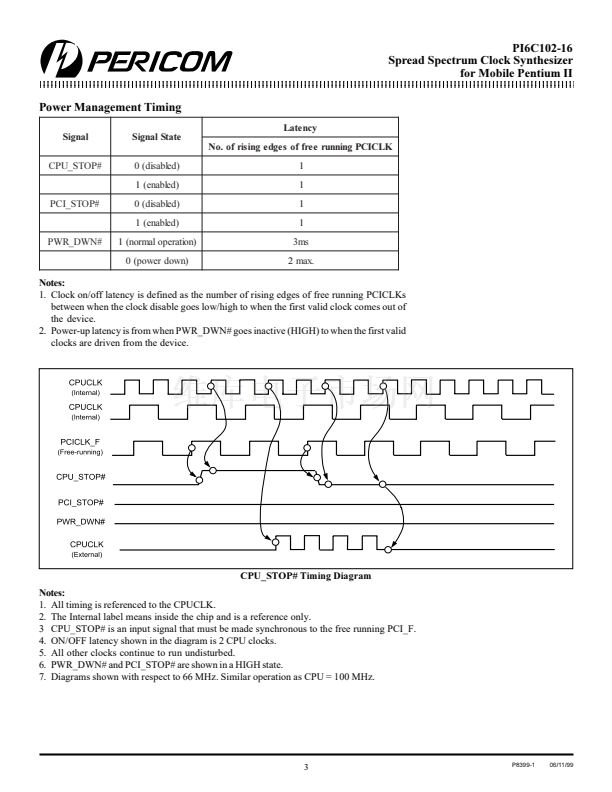
An asynchronous PWRDWN# signal may be used to orderly power
down (or up) the system.
PI6C102-16 is 鈥?.6% down spread, where as PI6C102-16B is
鹵0.75% center spread.
PI6C102-16D is the high drive version of PI6C102-16
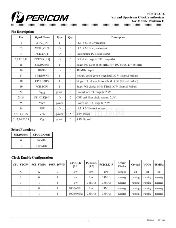
Block Diagram
Pin Configuration
XTAL_IN
1
2
3
4
5
6
7
8
9
10
11
12
13
14
28
27
26
25
24
VSS
VDD
REF
VDD2
CPUCLK0
CPUCLK1
VSS2
VDD
VSS
PCISTOP#
CPUSTOP#
PWRDWN#
48MHz
SEL100/66#
XTAL_IN
XTAL_OUT
PWRDWN#
REF
OSC
REF
XTAL_OUT
VSS
2 CPUCLK[0:1]
PLL1
SEL
100/66#
PLL2
CPUSTOP#
Div
PCISTOP#
PCICLK_F
梅2
48MHz
PCICLK_F
PCICLK1
VDD
5 PCICLK[1:5]
PCICLK2
PCICLK3
VDD
PCICLK4
PCICLK5
VSS
VDD
VSS
28-Pin
H
23
22
21
20
19
18
17
16
15
1
P8399-1
06/11/99


 1
1
 2
2
 3
3
 4
4
 5
5
 6
6
 7
7
 8
8
 9
9
 10
10
 11
11
 12
12
