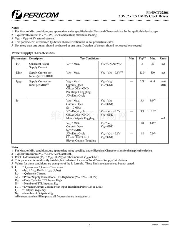
21098765432121098765432109876543210987654321210987654321098765432109876543212109876543210987654321098765432121098765432109876543210987654321
21098765432121098765432109876543210987654321210987654321098765432109876543212109876543210987654321098765432121098765432109876543210987654321
PI49FCT32806
3.3V, 2 x 1:5 CMOS Clock Driver
Features
聲
聲
聲
聲
聲
聲
聲
聲
聲
Low output skew: <270ps
Switching frequency of 133 MHz
Fast output rise/fall time <1.5ns
Low propagation delay <3.0ns
Low input capacitance <6.0pF
Balanced CMOS outputs
Industrial Temperature: 聳40擄C to +85擄C
3.3V 鹵10% operation
Packages available:
聳 20-pin 300-mil wide SOIC (S)
聳 20-pin 150-mil wide QSOP (Q)
聳 20-pin 209-mil wide SSOP (H)
Description
Pericom Semiconductor聮s PI49FCT series of logic circuits are
produced using the Company聮s advanced submicron CMOS
technology to achieve fast speed, low skew, fast slew rate, and low
propagation delay for most computing and communication
applications.
The PI49FCT32806 are inverting drivers. The outputs are configured
into 2 groups of 1-in, 5-out with independent output enable. Group
B has an extra MON output. Excellent output signals to power and
ground ratio minimize power and ground noise, and also improves
output performance.
PI49FCT32806 integrate series damping resistors on all outputs.
PI49FCT32806 Logic Block Diagram
OE
A
5
IN
A
OA
0鈥?
Product Pin Configuration
VCCA
OA0
OA1
OA2
5
IN
B
OE
B
OB
0鈥?
GNDA
OA3
OA4
GNDQ
OEA
MON
INA
1
2
3
4
20-Pin
5
H,Q,S
6
7
8
9
10
20
19
18
17
16
15
14
13
12
11
VCCB
OB0
OB1
OB2
GNDB
OB3
OB4
MON
OEB
INB
Product Pin Description
Pin Name
OE
A,
OE
B
IN
A,
IN
B
OA
N,
OB
N
MON
GND
V
CC
Description
Hi-Z State Output Enable Inputs (Active LOW)
Clock Inputs
Clock Outputs
Monitor Output
Ground
Power
Truth Table
(1)
Inputs
OE
A
, OE
B
L
L
H
H
IN
A
, IN
B
L
H
L
H
Outputs
OA
N
, OB
N
MON
H
H
L
L
Z
H
Z
L
Note:
1. H = High Voltage Level
Z = High Impedance
L = Low Voltage Level
1
PS8495
08/10/00


 1
1
 2
2
 3
3
 4
4
 5
5
 6
6
 7
7
