Philips Semiconductors
Product specification
PowerMOS transistor
PHP33N10
GENERAL DESCRIPTION
N-channel enhancement mode
field-effect power transistor in a
plastic envelope featuring stable
blocking voltage, fast switching and
high thermal cycling performance
with low thermal resistance. Intended
for use in Switched Mode Power
Supplies (SMPS), motor control
circuits and general purpose
switching applications.
QUICK REFERENCE DATA
SYMBOL
V
DS
I
D
P
tot
R
DS(ON)
PARAMETER
Drain-source voltage
Drain current (DC)
Total power dissipation
Drain-source on-state resistance
MAX.
100
34
175
0.057
UNIT
V
A
W
鈩?/div>
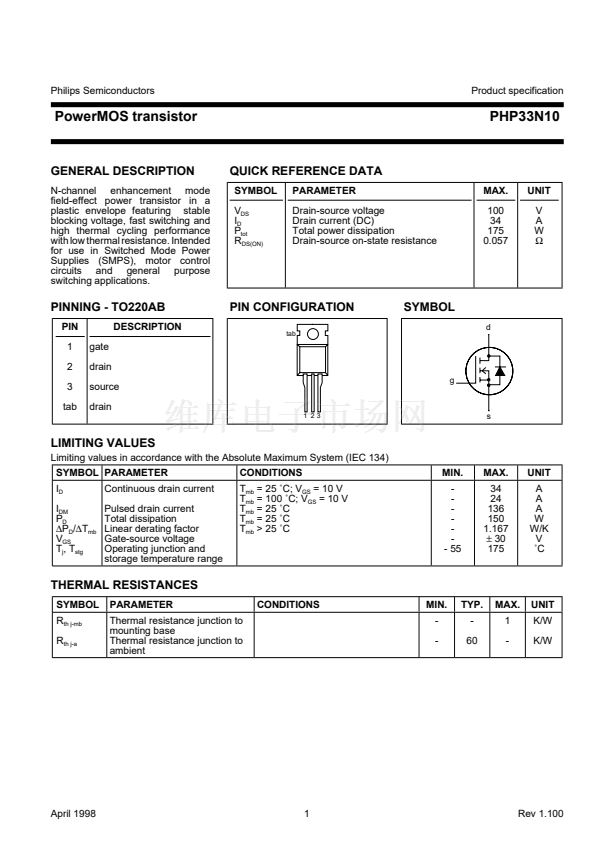
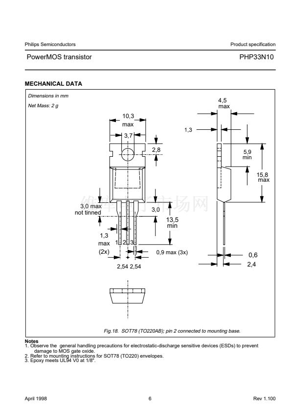
PINNING - TO220AB
PIN
1
2
3
tab
gate
drain
source
drain
DESCRIPTION
PIN CONFIGURATION
tab
SYMBOL
d
g
1 23
s
LIMITING VALUES
Limiting values in accordance with the Absolute Maximum System (IEC 134)
SYMBOL PARAMETER
I
D
I
DM
P
D
鈭哖
D
/鈭員
mb
V
GS
T
j
, T
stg
Continuous drain current
Pulsed drain current
Total dissipation
Linear derating factor
Gate-source voltage
Operating junction and
storage temperature range
CONDITIONS
T
mb
= 25 藲C; V
GS
= 10 V
T
mb
= 100 藲C; V
GS
= 10 V
T
mb
= 25 藲C
T
mb
= 25 藲C
T
mb
> 25 藲C
MIN.
-
-
-
-
-
-
- 55
MAX.
34
24
136
150
1.167
鹵
30
175
UNIT
A
A
A
W
W/K
V
藲C
THERMAL RESISTANCES
SYMBOL
R
th j-mb
R
th j-a
PARAMETER
Thermal resistance junction to
mounting base
Thermal resistance junction to
ambient
CONDITIONS
MIN.
-
-
TYP.
-
60
MAX.
1
-
UNIT
K/W
K/W
April 1998
1
Rev 1.100


 1
1
 2
2
 3
3
 4
4
 5
5
 6
6
 7
7
