鈥?/div>
General Description
The PEEL22LV10AZ is a Programmable Electrically
Erasable Logic (PEEL) SPLD (Simple Programmable
Logic Device) that operates over the supply voltage
range of 2.7V-3.6V and features ultra-low, automatic
"zero" power-down operation. The PEEL22LV10AZ is
logically and functionally similar to ICT's 5V
PEEL22CV10A and PEEL22CV10AZ. The "zero power"
(25
碌A(chǔ)
max. I
CC
) power-down mode makes the
PEEL22LV10AZ ideal for a broad range of battery-
powered portable equipment applications, from hand-
held
meters
to
PCMCIA
modems.
EE-
reprogrammability provides both the convenience of
product fast reprogramming for product development
and quick personalization in manufacturing, including
Engineering Change Orders.
Figure 1 - Pin Configuration
I/CLK
I
I
I
I
I
I
I
I
I
I
G ND
1
2
3
4
5
6
7
8
9
10
11
12
24
23
22
21
20
19
18
17
16
15
14
13
VCC
I/O
I/O
I/O
I/O
I/O
I/O
I/O
I/O
I/O
I/O
I
I/CLK
I
I
I
I
I
I
I
I
I
I
G ND
1
2
3
4
5
6
7
8
9
10
11
12
24
23
22
21
20
19
18
17
16
15
14
13
VCC
I/O
I/O
I/O
I/O
I/O
I/O
I/O
I/O
I/O
I/O
I
The differences between the PEEL22LV10AZ and
PEEL22CV10A include the addition of programmable
clock polarity, p-term clock, and Schmitt trigger input
buffers on all inputs, including the clock. Schmitt trigger
inputs allow direct input of slow signals such as
biomedical and sine waves or clocks. Like the
PEEL22CV10A, the PEEL22LV10AZ is a pin and
JEDEC compatible, logical superset of the industry
standard
PAL22V10
SPLD
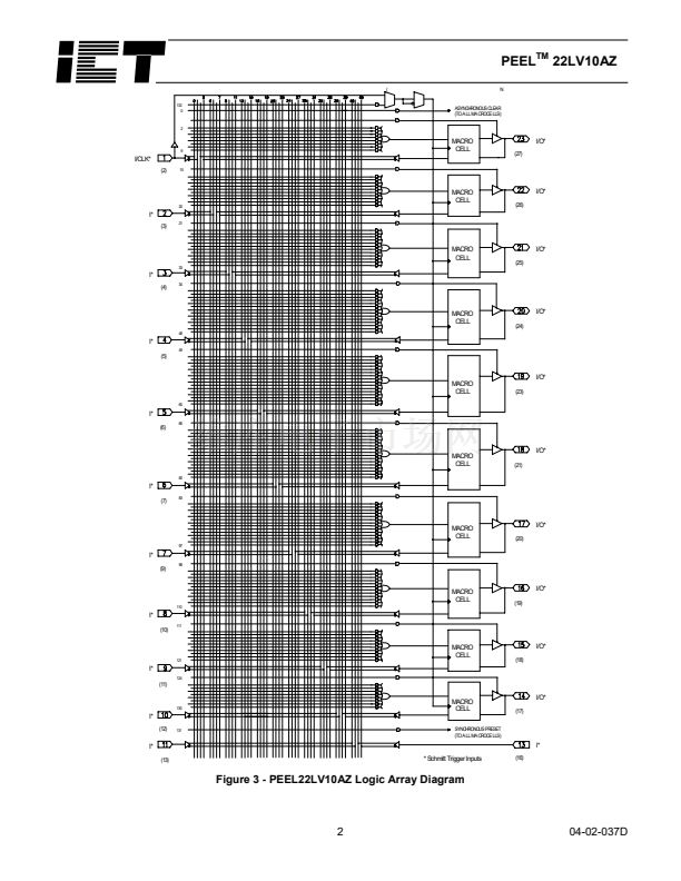
Figure
1.
The
PEEL22LV10AZ provides additional architectural
features that allow more logic to be incorporated into
the design. The PEEL22LV10AZ architecture allows it
to replace over twenty standard 24-pin DIP, SOIC,
TSSOP
and
PLCC
packages.
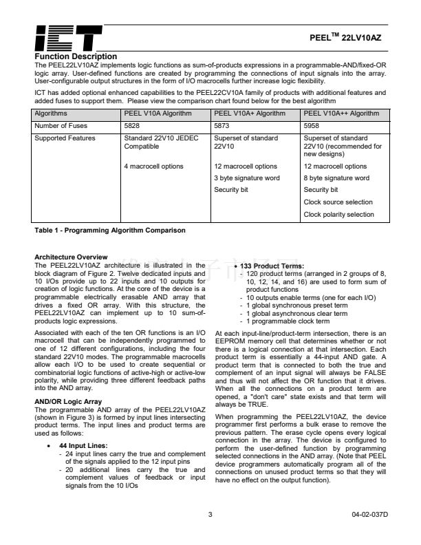
Figure 2 - Block Diagram
CLK MUX (O ptiona l)
I
I
I
NC
I
I
I
4 3 2 1 28 27 26
5
25
6
24
7
23
8
22
9
21
10
20
11
19
12 13 14 15 16 17 18
I
I
I/CLK
NC
VCC
I/O
I/O
DIP
TSSOP
I/CLK
I
I
I
I
I
I
I
I
I
I
I
SP
AC
PEEL
T M
"AND"
ARRAY
OE
MACRO
CEL L
I/O
I/O
I/O
I/O
I/O
I/O
I/O
I/O
I/O
I/O
133 Terms
X
44 Inp uts
I/O
I/O
I/O
NC
I/O
I/O
I/O
I
I
G ND
NC
I
I/O
I/O
I/CLK
I
I
I
I
I
I
I
I
I
I
G ND
1
2
3
4
5
6
7
8
9
10
11
12
24
23
22
21
20
19
18
17
16
15
14
13
VCC
I/O
I/O
I/O
I/O
I/O
I/O
I/O
I/O
I/O
I/O
I
SP = SYNCHRONO US PRESET
AC = ASYNCHRONO US CLEAR
O E = O UTPUT ENABLE
PLCC
SOIC
1
04-02-037D


 1
1
 2
2
 3
3
 4
4
 5
5
 6
6
 7
7
 8
8
 9
9
 10
10
