鈥?/div>
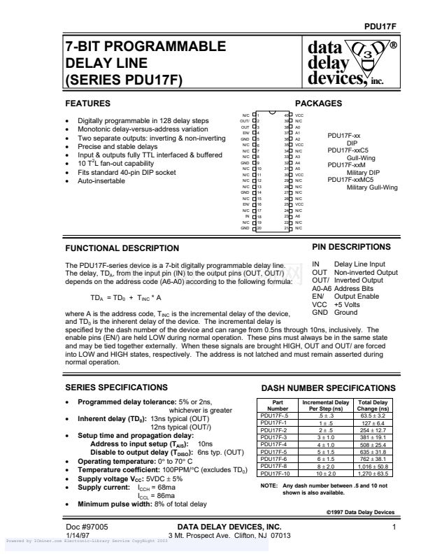
N/C
1
2
3
4
5
6
7
8
9
10
11
12
13
14
15
16
17
18
19
20
40
39
38
37
36
35
34
33
32
31
30
29
28
27
26
25
24
23
22
21
VCC
N/C
A0
A1
A2
VCC
N/C
A3
A4
A5
VCC
N/C
N/C
N/C
N/C
VCC
N/C
A6
N/C
N/C
data
3
廬
delay
devices,
inc.
PACKAGES
OUT/
OUT
EN/
GND
N/C
N/C
N/C
GND
N/C
N/C
N/C
N/C
GND
N/C
EN/
N/C
IN
N/C
GND
Digitally programmable in 128 delay steps
Monotonic delay-versus-address variation
Two separate outputs: inverting & non-inverting
Precise and stable delays
Input & outputs fully TTL interfaced & buffered
10 T
2
L fan-out capability
Fits standard 40-pin DIP socket
Auto-insertable
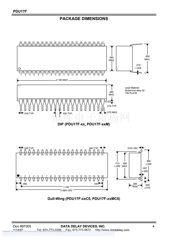
PDU17F-xx
DIP
PDU17F-xxC5
Gull-Wing
PDU17F-xxM
Military DIP
PDU17F-xxMC5
Military Gull-Wing
FUNCTIONAL DESCRIPTION
The PDU17F-series device is a 7-bit digitally programmable delay line.
The delay, TD
A
, from the input pin (IN) to the output pins (OUT, OUT/)
depends on the address code (A6-A0) according to the following formula:
TD
A
= TD
0
+ T
INC
* A
PIN DESCRIPTIONS
IN
OUT
OUT/
A0-A6
EN/
VCC
GND
Delay Line Input
Non-inverted Output
Inverted Output
Address Bits
Output Enable
+5 Volts
Ground
where A is the address code, T
INC
is the incremental delay of the device,
and TD
0
is the inherent delay of the device. The incremental delay is
specified by the dash number of the device and can range from 0.5ns through 10ns, inclusively. The
enable pins (EN/) are held LOW during normal operation. These pins must always be in the same state
and may be tied together externally. When these signals are brought HIGH, OUT and OUT/ are forced
into LOW and HIGH states, respectively. The address is not latched and must remain asserted during
normal operation.
SERIES SPECIFICATIONS
鈥?/div>
鈥?/div>
鈥?/div>
鈥?/div>
鈥?/div>
鈥?/div>
鈥?/div>
鈥?/div>
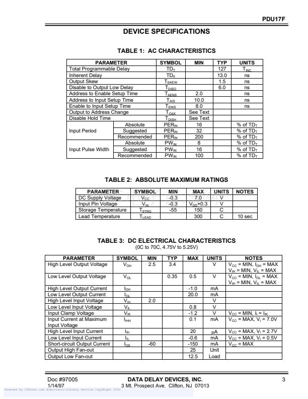
Programmed delay tolerance:
5% or 2ns,
whichever is greater
Inherent delay (TD
0
):
13ns typical (OUT)
12ns typical (OUT/)
Setup time and propagation delay:
Address to input setup (T
AIS
):
10ns
Disable to output delay (T
DISO
):
6ns typ. (OUT)
Operating temperature:
0擄 to 70擄 C
Temperature coefficient:
100PPM/擄C (excludes TD
0
)
Supply voltage V
CC
:
5VDC
鹵
5%
Supply current:
I
CCH
= 68ma
I
CCL
= 86ma
Minimum pulse width:
8% of total delay
DASH NUMBER SPECIFICATIONS
Part
Number
PDU17F-.5
PDU17F-1
PDU17F-2
PDU17F-3
PDU17F-4
PDU17F-5
PDU17F-6
PDU17F-8
PDU17F-10
Incremental Delay
Per Step (ns)
.5
鹵
.3
1
鹵
.5
2
鹵
.5
3
鹵
1.0
4
鹵
1.0
5
鹵
1.5
6
鹵
1.5
8
鹵
2.0
10
鹵
2.0
Total Delay
Change (ns)
63.5
鹵
3.2
127
鹵
6.4
254
鹵
12.7
381
鹵
19.1
508
鹵
25.4
635
鹵
31.8
762
鹵
38.1
1,016
鹵
50.8
1,270
鹵
63.5
NOTE: Any dash number between .5 and 10 not
shown is also available.
漏
1997 Data Delay Devices
Doc #97005
1/14/97
Powered by ICminer.com Electronic-Library Service CopyRight 2003
DATA DELAY DEVICES, INC.
3 Mt. Prospect Ave. Clifton, NJ 07013
1
PDU17F-10M相關型號PDF文件下載
-
型號
版本
描述
廠商
下載
-
英文版
3-BIT PROGRAMMABLE
DELAY LINE
DATA DELAY DEVI...
-
英文版
Programmable 3-bit TTL delay line
ETC
-
英文版
3-BIT PROGRAMMABLE
DELAY LINE
DATA DELAY DEVI...
-
英文版
4-BIT PROGRAMMABLE DELAY LINE
ETC
-
英文版
4-BIT PROGRAMMABLE
DELAY LINE
DATA DELAY DEVI...
-
英文版
4-BIT PROGRAMMABLE DELAY LINE
-
英文版
Programmable 5-bit TTL delay line
ETC
-
英文版
5-BIT PROGRAMMABLE
DELAY LINE
DATA DELAY DEVI...
-
英文版
Programmable 6-bit TTL delay line
ETC
-
英文版
6-BIT PROGRAMMABLE
DELAY LINE
DATA DELAY DEVI...
-
英文版
Programmable 7-bit TTL delay line
ETC
-
英文版
7-BIT PROGRAMMABLE
DELAY LINE
DATA DELAY DEVI...
-
英文版
Programmable 8-bit TTL delay line
ETC
-
英文版
8-BIT PROGRAMMABLE
DELAY LINE
DATA DELAY DEVI...
-
英文版
Programmable 3-bit 10K ECL delay line
ETC
-
英文版
3-BIT, ECL-INTERFACED
PROGRAMMABLE DELAY LINE
DATA DELAY DEVI...
-
英文版
Power Outlet Strip; No. of Outlets:13; Outlet Type:NEMA 5-15...
-
英文版
POWER STRIP 20A 13 OUT RACK MNT
-
英文版
Power Outlet Strip; Supply Voltage:120VAC; No. of Outlets:13...
-
英文版
Suppressor; Suppressor Type:Outlet Strip; No. of Outlets:14;...


 1
1
 2
2
 3
3
 4
4
 5
5
