PA7536 PEEL Array鈩?/div>
Programmable Electrically Erasable Logic Array
Versatile Logic Array Architecture
- 12 I/Os, 14 inputs, 36 registers/latches
- Up to 36 logic cell output functions
- PLA structure with true product-term sharing
- Logic functions and registers can be I/O-buried
Ideal for Combinatorial, Synchronous and
Asynchronous Logic Applications
- Integration of multiple PLDs and random logic
- Buried counters, complex state-machines
- Comparators, decoders, multiplexers and
other wide-gate functions
High-Speed Commercial and Industrial Versions
- As fast as 9ns/15ns (tpdi/tpdx), 83.3MHz (f
MAX
)
- Industrial grade available for 4.5 to 5.5V V
CC
and
-40 to +85 擄C temperatures
CMOS Electrically Erasable Technology
- Reprogrammable in 28-pin DIP, SOIC and PLCC
packages
Flexible Logic Cell
- Up to 3 output functions per logic cell
- D,T and JK registers with special features
- Independent or global clocks, resets, presets,
clock polarity and output enables
- Sum-of-products logic for output enables
Development and Programmer Support
- ICT WinPLACE Development Software
- Fitters for ABEL, CUPL and other software
- Programming support by popular third-party
programmer
General Description
The PA7536 is a member of the Programmable Electrically
Erasable Logic (PEEL鈩? Array family based on ICT鈥檚
CMOS EEPROM technology. PEEL鈩?Arrays free
designers from the limitations of ordinary PLDs by
providing the architectural flexibility and speed needed for
today鈥檚 programmable logic designs. The PA7536 offers
versatile logic array architecture with 12 I/O pins, 14 input
pins and 36 registers/latches (12 buried logic cells, 12
Input registers/latches and 12 buried registers/latches). Its
logic array implements 50 sum-of-products logic functions
that share 64 product terms. The PA7536鈥檚 logic and I/O
cells (LCCs, IOCs) are extremely flexible offering up to
three output functions per cell (a total of 36 for all 12 logic
cells). Cells are configurable as D, T, and JK registers with
independent or global clocks, resets, presets, clock
polarity, and other special features, making the PA7536
suitable for a variety of combinatorial, synchronous and
asynchronous logic applications. The PA7536 offers pin
compatibility and super-set functionality to popular 28-pin
PLDs, such as the 26V12. Thus, designs that exceed the
architectures of such devices can be expanded upon. The
PA7536 supports speeds as fast as 9ns/15ns (tpdi/tpdx)
and 83.3MHz (f
MAX
) and moderate power consumption
60mA (45mA typical). Packaging includes 28-pin DIP,
SOIC, and PLCC (see Figure 1). Development and
programming support for the PA7536 is provided by ICT
and popular third-party development tool manufacturers.
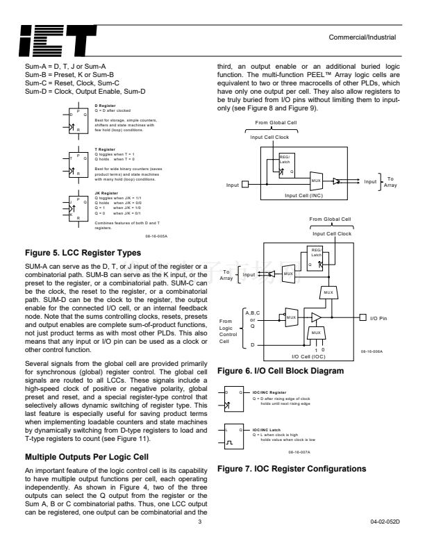
Figure 1. Pin Configuration
I/C LK1
I
I
I
I
I
VC C
I
I
I
I
I
I
I
1
2
3
4
5
6
7
8
9
10
11
12
13
14
28
27
26
25
24
23
22
21
20
19
18
17
16
15
I/C LK2
I/O
I/O
I/O
I/O
I/O
I/O
G ND
I/O
I/O
I/O
I/O
I/C LK1
I/O
I/O
I
I
I
I/C LK2
I/C LK1
I
I
I
I
I
VC C
I
I
I
I
I
I
I
1
2
3
4
5
6
7
8
9
10
11
12
13
14
28
27
26
25
24
23
22
21
20
19
18
17
16
15
I/C LK2
I/O
I/O
I/O
I/O
I/O
I/O
G ND
I/O
I/O
I/O
I/O
I/O
I/O
Figure 2. Block Diagram
2 Input/
G lobal C lock Pins
G lobal
C ells
12 Input P ins
Input
Cells
(IN C )
2
76 (38X 2)
A rray Inputs
true and
com plem ent
I/O
C ells
(IO C )
Buried
logic
Logic functions
to I/O cells
12 I/O Pins
12
12
S O IC /TS S O P
I/O
I/O
12
I/CL K1
I
I
I
I/O Ce lls
In p ut C ells
G lo ba l Ce lls
I/CL K2
I/O
I/O
I/O
I/O
I/O
I/O
G ND
I/O
I/O
I/O
L og ic Co ntro l C e lls
I/O
I/O
L og ic
Array
D IP
4
I
I
VC C
I
I
I
I
5
6
7
8
9
10
11
12 13 14 15 16 17 18
3
2
1 28 27 26
25
24
23
22
21
20
19
I/O
I/O
I/O
I/O
G ND
I/O
I/O
I
I
VC C
I
I
I
I
I
I
I
A
B
C
D
Logic
C ontrol
C ells
(LC C )
12
2 sum term s
3 product term s
for G lobal C ells
12
48 sum term s
(four per LC C )
12 Logic C ontrol Cells
up to 3 output functions per cell
(36 total output functions possible)
P A7536
I/O
0 8-1 6-0 02 A
I/O
I/O
I/O
I/O
PLCC
08-16-001A
I
I
I
1
04-02-052D


 1
1
 2
2
 3
3
 4
4
 5
5
 6
6
 7
7
 8
8
 9
9
 10
10
