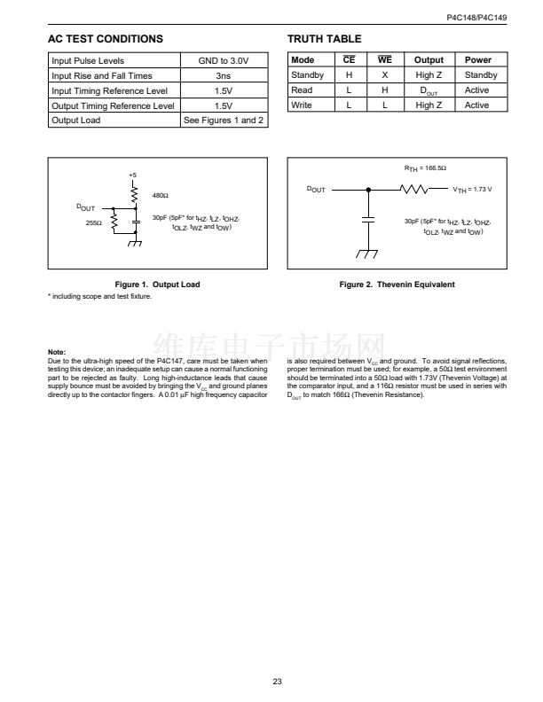
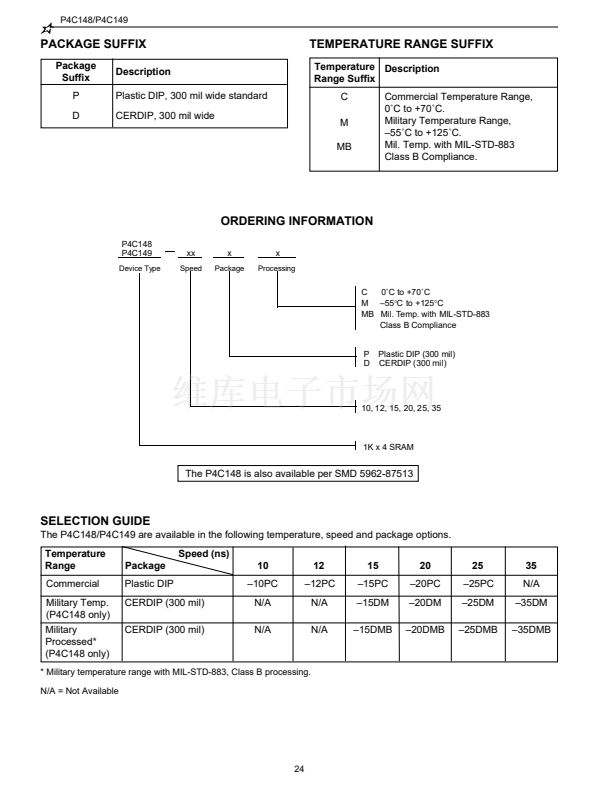
P4C148, P4C149
ULTRA HIGH SPEED 1K x 4
STATIC CMOS RAMS
FEATURES
Full CMOS, 6T Cell
High Speed (Equal Access and Cycle Times)
鈥?10/12/15/20/25 ns (Commercial)
鈥?15/20/25/35 ns (P4C148 Military)
Low Power Operation
鈥?715 mW Active
鈥?0 (Commecial)
鈥?550 mW Active
鈥?5 (Commercial)
鈥?110 mW Standby (TTL Input) P4C148
鈥?55 mW Standby (CMOS Input) P4C148
Single 5V
鹵
10% Power Supply
P4C148/P4C149
Two Options
鈥?P4C148 Low Power Standby Mode
鈥?P4C149 Fast Chip Select Control
Common Input/Output Ports
Three-State Outputs
Fully TTL Compatible Inputs and Outputs
Standard Pinout (JEDEC Approved)
鈥?18 Pin 300 mil DIP
DESCRIPTION
The P4C148 and P4C149 are 4,096-bit ultra high-speed
static RAMs organized as 1K x 4. Both devices have
common input/output ports. The P4C148 enters the standby
mode when the chip enable (CE) goes HIGH; with CMOS
input levels, power consumption is extremely low in this
mode. The P4C149 features a fast chip select capability
using
CS.
The CMOS memories require no clocks or
refreshing, and have equal access and cycle times. Inputs
are fully TTL-compatible. The RAMs operate from a single
5V
鹵
10% tolerance power supply.
Access times as fast as 10 nanoseconds are available,
permitting greatly enhanced system operating speeds.
CMOS is used to reduce power consumption when active;
for the P4C148, consumption is further reduced in the
standby mode.
The P4C148 and P4C149 are available in 18-pin 300 mil
DIP packages providing excellent board level densities.
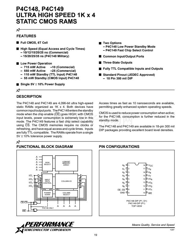
FUNCTIONAL BLOCK DIAGRAM
A
A
A
A
A
A
I/O
1
I/O
2
I/O
3
I/O
4
INPUT
DATA
CONTROL
COLUMN I/O
PIN CONFIGURATIONS
ROW
SELECT
4,096-BIT
MEMORY
ARRAY
A0
A1
A2
A3
A4
A5
A6
CE, CS
GND
1
2
3
4
5
6
7
8
9
18
17
16
15
14
13
12
11
10
V CC
A9
A8
A7
I/O4
I/O3
I/O2
I/O1
WE
POWER
DOWN
COLUMN
SELECT
CE/CS
A
P4C148 ONLY
A
A
A
P4C148 DIP (P1, D1)
P4C149 DIP (P1)
TOP VIEW
WE
Means Quality, Service and Speed
1Q97
19


 1
1
 2
2
 3
3
 4
4
 5
5
 6
6
