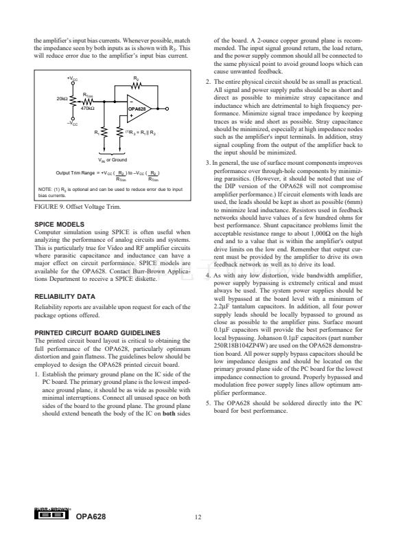
鈭?/div>
Hz
q
LOW NOISE FIGURE: 9dB
q
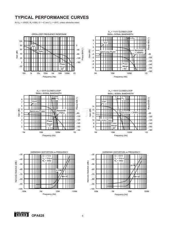
BANDWIDTH (Gain = +1): 160MHz
q
0.1dB GAIN FLATNESS: 30MHz
q
LOW OFFSET VOLTAGE: 500
碌
V
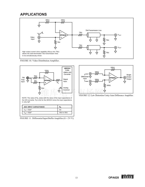
APPLICATIONS
q
BROADCAST QUALITY VIDEO
q
MEDICAL IMAGING
q
LOW NOISE PREAMPLIFIER
q
PRECISION ADC/DAC BUFFER
q
TELECOMMUNICATIONS
q
ANALYTICAL INSTRUMENTS
q
ACTIVE FILTERS
q
DC RESTORATION CIRCUITS
DESCRIPTION
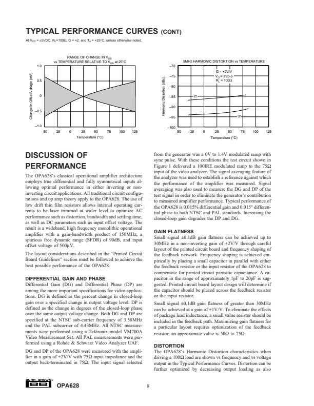
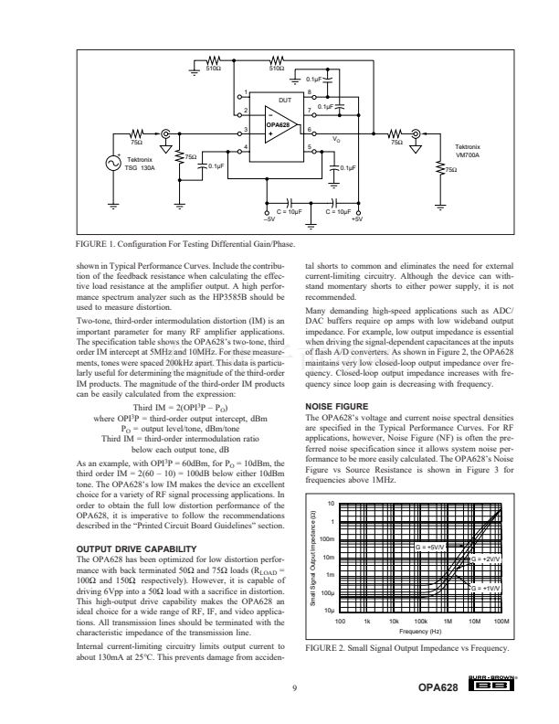
The OPA628 is a low distortion, wideband operational
amplifier. It features low differential gain error of
0.015% and low differential phase error of 0.015擄 at
NTSC and PAL frequencies with a 150鈩?load (a back-
terminated 75鈩?cable). The 0.1dB gain flatness to
30MHz, and the excellent differential gain and phase
make the OPA628 ideal for broadcast quality video
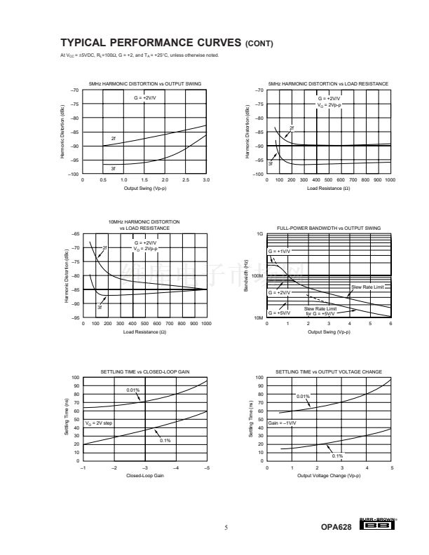
applications. In addition, the spurious free dynamic
range of 90dB makes the OPA628 an excellent choice
to buffer the input of precision Analog-to-Digital con-
verters. It can also be used to provide a buffer for the
output of precision high speed Digital-to-Analog con-
verters. The two-tone third-order intercept of the
OPA628 is 60dBm.
The OPA628 is a unity gain stable, voltage feedback
operational amplifier. It has all of the benefits asso-
ciated with voltage feedback amplifiers including
high input impedance, high common mode rejection,
and symmetrical differential input flexibility. The
unity gain bandwidth of the OPA628 is 160MHz. The
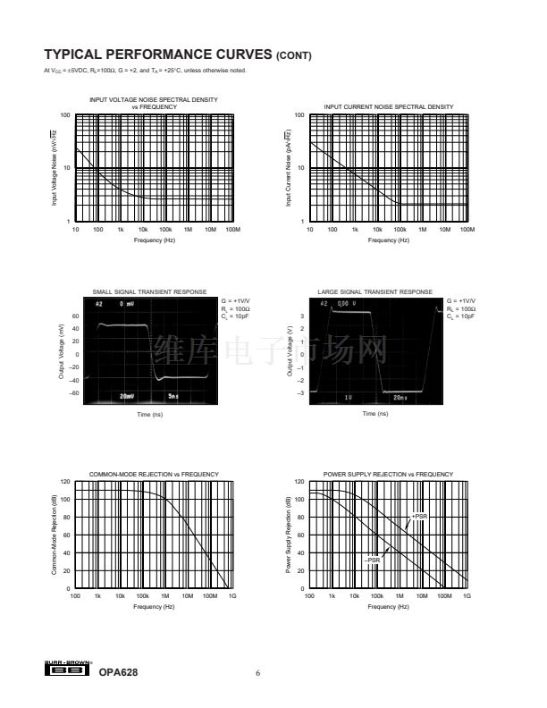
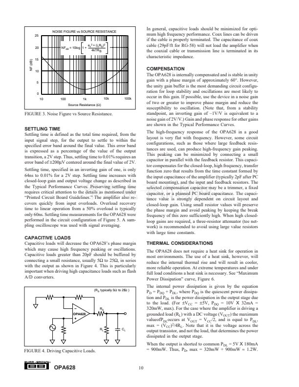
low noise of 2.5nV/鈭欻z and low noise figure of 9dB
(R
S
= 50鈩? make the OPA628 very useful in preci-
sion applications requiring wide dynamic range.
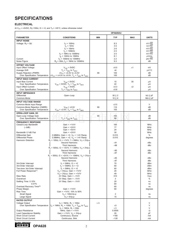
The superior distortion performance of the OPA628 is
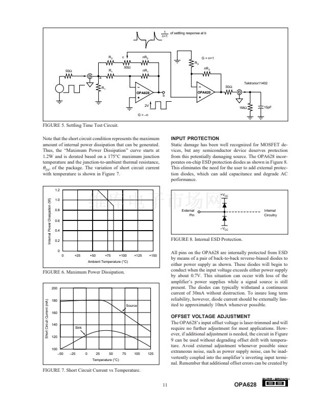
achieved by its multistage architecture which provides
high open-loop gain. The distortion performance is
additionally enhanced by separating the power sup-
plies to the input and output stages requiring four
power supply connections as shown in the block
diagram below. This separation of supplies eliminates
the effects of package and wire bond parasitic capaci-
tance and inductance. The OPA628 is powered with
鹵5VDC
supplies for low power dissipation. The
OPA628 is available in 8-pin SOIC package. The
temperature range is 鈥?0擄C to +85擄C.
+V
CC
, Input Stage
8
Active
Load
+V
CC
, Output Stage
7
Non-Inverting
Input
3
+1
6
Output
2
Inverting
Input
5
4
鈥揤
CC
, Input Stage
鈥揤
CC
, Output Stage
International Airport Industrial Park 鈥?Mailing Address: PO Box 11400, Tucson, AZ 85734 鈥?Street Address: 6730 S. Tucson Blvd., Tucson, AZ 85706 鈥?Tel: (520) 746-1111 鈥?Twx: 910-952-1111
Internet: http://www.burr-brown.com/ 鈥?FAXLine: (800) 548-6133 (US/Canada Only) 鈥?Cable: BBRCORP 鈥?Telex: 066-6491 鈥?FAX: (520) 889-1510 鈥?Immediate Product Info: (800) 548-6132
廬
漏
1993 Burr-Brown Corporation
PDS-1204B
1
Printed in U.S.A. March, 1998
OPA628


 1
1
 2
2
 3
3
 4
4
 5
5
 6
6
 7
7
 8
8
 9
9
 10
10
 11
11
 12
12
 13
13
