Transmissive Photosensors (Photo Interrupters)
ON1110
Photo Interrupter
For contactless SW, object detection
Outline
ON1110 is a photocoupler in which a high efficiency GaAs
infrared light emitting diode is used as the light emitting element,
and a high sensitivity phototransistor is used as the light detecting
element. The two elements are arranged so as to face each other,
and objects passing between them are detected.
1.6
Unit : mm
Mark for indicating
LED side
2.0
酶1.2
3.0鹵0.3
2.0鹵0.2
13.8鹵0.3
2.8鹵0.2
A
0.4鹵0.1
8.8鹵0.2
0.5
Features
Highly precise position detection : 0.3 mm
Fast response : t
r
, t
f
= 6
碌s
(typ.)
Small output current variation against change in temperature
Small package used for saving mounting space
Device
center
A'
3.0
*10.0鹵0.4
3
2
4
1
0.5
1.8鹵0.2
8.0 min.
2
0.8
6.0鹵0.2
4.0
1.6
,,
,,
0.7
*2.54
SEC. A-A'
3
4
Absolute Maximum Ratings
(Ta = 25藲C)
Parameter
Reverse voltage (DC)
Input (Light
Forward current (DC)
emitting diode)
Power dissipation
Collector current
Symbol Ratings
V
R
I
F
P
D*1
I
C
3
50
75
20
30
5
100
Unit
V
mA
mW
mA
V
V
mW
藲C
藲C
*1
1
Pin connection
(Note) * is dimension at the root of leads
Output (Photo Collector to emitter voltage V
CEO
transistor)
Emitter to collector voltage V
ECO
Collector power dissipation
Temperature
Operating ambient temperature
Storage temperature
P
C*2
T
opr
鈥?5 to +85
T
stg
鈥?0 to +100
Input power derating ratio is
1.0 mW/藲C at Ta
鈮?/div>
25藲C.
*2
Output power derating ratio is
1.33 mW/藲C at Ta
鈮?/div>
25藲C.
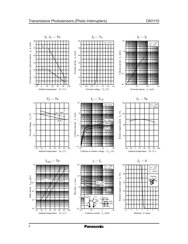
Electrical Characteristics
(Ta = 25藲C)
Parameter
Forward voltage (DC)
Input
Reverse current (DC)
characteristics
Capacitance between terminals
Collector cutoff current
Output
characteristics Collector to emitter capacitance
Symbol
V
F
I
R
C
t
I
CEO
C
C
V
R
= 3V
V
R
= 0V, f = 1MHz
V
CE
= 10V
V
CE
= 10V, f = 1MHz
0.3
6
0.3
5
50
200
Conditions
I
F
= 50mA
min
typ
1.2
max
1.5
10
Unit
V
碌A
pF
nA
pF
mA
碌s
V
Collector current
I
C*2
V
CE
= 10V, I
F
= 20mA
Transfer
Response time
t
r
, t
f*1
V
CC
= 10V, I
C
= 1mA, R
L
= 100鈩?/div>
characteristics
Collector to emitter saturation voltage V
CE(sat)
I
F
= 50mA, I
C
= 0.1mA
*
Switching time measurement circuit
Sig.IN
V
CC
(Input pulse)
Sig.OUT (Output pulse)
90%
10%
t
d
t
r
t
f
t
d
: Delay time
t
r
: Rise time (Time required for the collector current to increase
from 10% to 90% of its final value)
t
f
: Fall time (Time required for the collector current to decrease
from 90% to 10% of its initial value)
*2
I
C
classifications
Class
I
C
(mA)
,,
Q
,,
50鈩?/div>
R
L
R
0.75 to 2.15
S
> 1.85
0.3 to 0.85
1


 1
1
 2
2
