-
-

- 手機(jī)版
-

- 芯視頻 APP
-

- 微信公眾號(hào)
-

- 維庫(kù)官方抖音
-

- 微信頭條號(hào)
-
- |
-
- |
- |
- |

掃碼查看芯片數(shù)據(jù)手冊(cè)
上傳產(chǎn)品規(guī)格書(shū)
ON Semiconductor
門(mén)(與/非與/或/非或)
NOR
NL27WZ
2
2 / 1
- 32 mA
32 mA
4.8 ns
5.5 V
1.65 V
+ 85 C
SMD/SMT
US
Reel
- 40 C
2
1
3000


聯(lián)系人:
聯(lián)系方式:

 1
1
 2
2
 3
3
 4
4
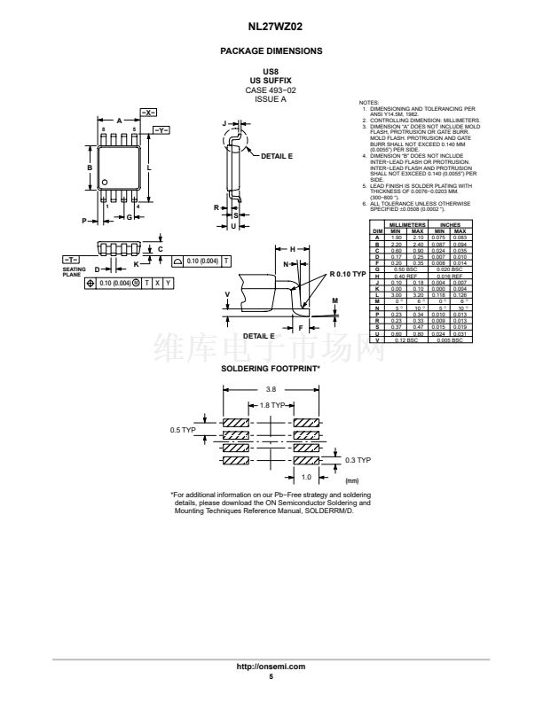 5
5
 6
6
