PRELIMINARY DATA SHEET
N-CHANNEL GaAs HJ-FET
NE6510379A
3 W L-BAND POWER GaAs HJ-FET
DESCRIPTION
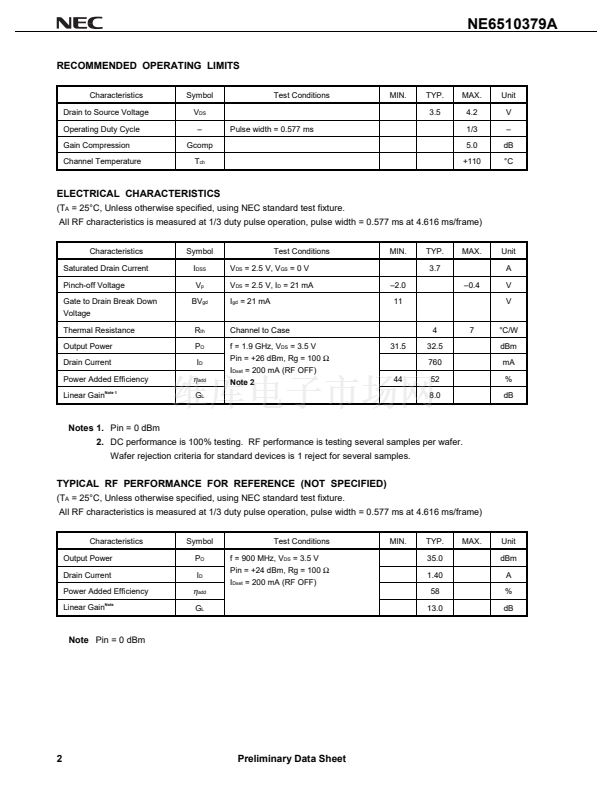
The NE6510379A is a 3 W GaAs HJ-FET designed for middle power transmitter applications for mobile
communication systems. It is capable of delivering 3 watt of output power (1/3 Duty pulse operation) with high linear
gain, high efficiency and excellent distortion.
Reliability and performance uniformity are assured by NEC鈥檚 stringent quality and control procedures.
FEATURES
鈥?GaAs HJ-FET Structure
鈥?High Output Power
鈥?High Linear Gain
: P
O
= +35 dBm typ. @V
DS
= 3.5 V, I
Dset
= 200 mA, f = 900 MHz, Pin = +24 dBm, 1/3 duty
P
O
= +32.5 dBm typ. @V
DS
= 3.5 V, I
Dset
= 200 mA, f = 1.9 GHz, Pin = +26 dBm, 1/3 duty
: G
L
= 13 dB typ. @V
DS
= 3.5 V, I
Dset
= 200 mA, f = 900 MHz, Pin = 0 dBm, 1/3 duty
G
L
= 8 dB typ. @V
DS
= 3.5 V, I
Dset
= 200 mA, f = 1.9 GHz, Pin = 0 dBm, 1/3 duty
鈥?High Power Added Efficiency: 58% typ. @V
DS
= 3.5 V, I
Dset
= 200 mA, f = 900 MHz, Pin = +24 dBm, 1/3 duty
52% typ. @V
DS
= 3.5 V, I
Dset
= 200 mA, f = 1.9 GHz, Pin = +26 dBm, 1/3 duty
ORDERING INFORMATION (PLAN)
Part Number
NE6510379A-T1
79A
Package
Supplying Form
12 mm tape width, 1 kpcs/reel
Remark
To order evaluation samples, please contact your local NEC sales office.
(Part number for sample order: NE6510379A)
ABSOLUTE MAXIMUM RATINGS (T
A
= 25擄C)
Operation in excess of any one of these parameters may result in permanent damage.
Parameter
Drain to Source Voltage
Gate to Source Voltage
Drain Current
Gate Forward Current
Gate Reverse Current
Total Power Dissipation
Channel Temperature
Storage Temperature
Symbol
V
DS
V
GSO
I
D
I
GF
I
GR
P
T
T
ch
T
stg
Ratings
6
鈥?
4.2
38
38
18
150
鈥?5 to +150
Unit
V
V
A
mA
mA
W
擄C
擄C
Caution
Please handle this device at static-free workstation, because this is an electrostatic sensitive
device.
The information in this document is subject to change without notice.
Document No. P13677EJ1V0DS00 (1st edition)
Date Published August 1998 N CP(K)
Printed in Japan
漏
1998


 1
1
 2
2
 3
3
 4
4
 5
5
 6
6
 7
7
 8
8
