ULTRA LOW NOISE
PSEUDOMORPHIC HJ FET
NOT RECOMMENDED FOR NEW DESIGN
NE32684A
FEATURES
鈥?VERY LOW NOISE FIGURE:
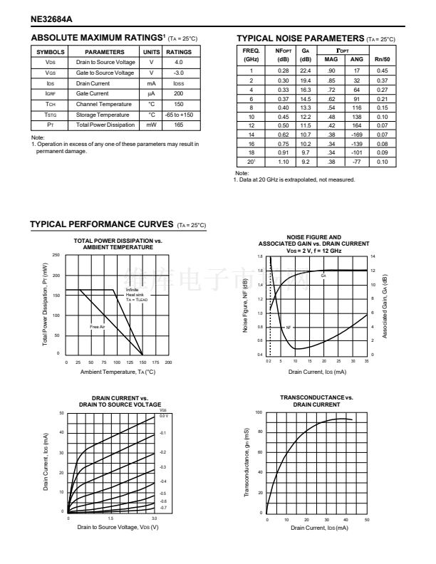
0.5 dB typical at 12 GHz
Noise Figure, NF (dB)
1.2
NOISE FIGURE & ASSOCIATED
GAIN vs. FREQUENCY
V
DS
= 2 V, I
DS
= 10 mA
24
GA
碌m,
W
G
= 200
碌
m
鈥?L
G
= 0.20
碌
鈥?LOW COST METAL CERAMIC PACKAGE
鈥?TAPE & REEL PACKAGING OPTION AVAILABLE
0.8
18
0.6
15
0.4
NF
0.2
12
DESCRIPTION
The NE32684A is a pseudomorphic Hetero-Junction FET that
uses the junction between Si-doped AlGaAs and undoped
InGaAs to create very high mobility electrons. The device
features mushroom shaped TiAl gates for decreased gate
resistance and improved power handling capabilities. The
mushroom gate also results in lower noise figure and high
associated gain. This device is housed in an epoxy-sealed,
metal/ceramic package and is intended for high volume con-
sumer and industrial applications.
NEC's stringent quality assurance and test procedures assure
the highest reliability and performance.
9
0
1
10
30
6
Frequency, f (GHz)
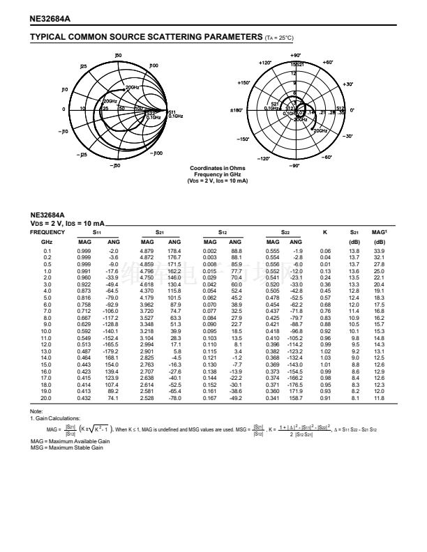
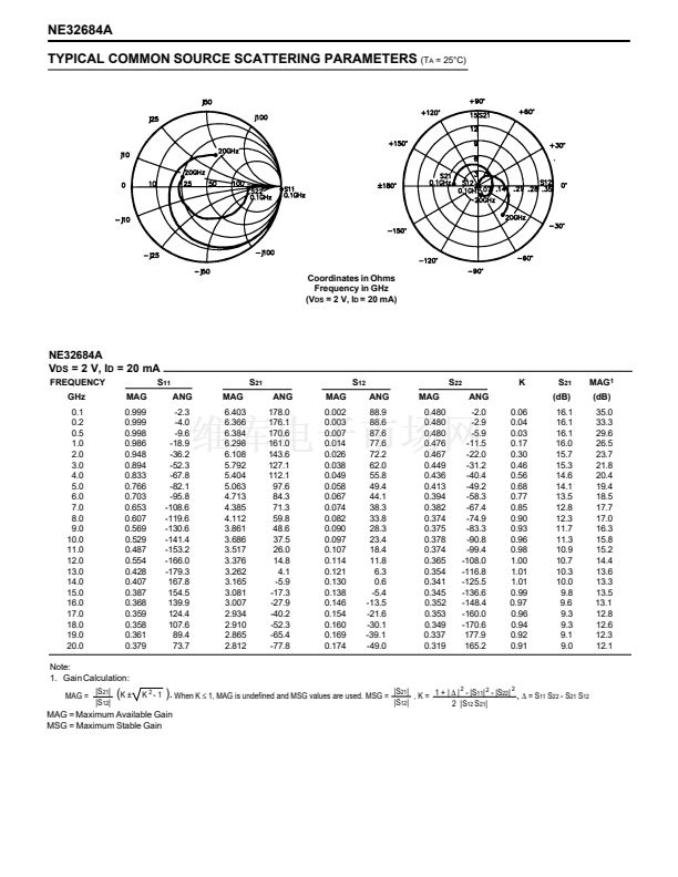
ELECTRICAL CHARACTERISTICS
(T
A
= 25擄C)
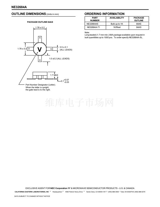
PART NUMBER
PACKAGE OUTLINE
SYMBOLS
NF
1
NE32684A
84AS
UNITS
dB
dB
dBm
dBm
dB
dB
mA
V
mS
碌A
擄C/W
擄C/W
15
-2.0
45
10.0
MIN
TYP
0.5
11.5
8.5
10.75
11.0
11.5
40
-0.8
60
0.5
750
350
10.0
70
-0.2
MAX
0.6
PARAMETERS AND CONDITIONS
Optimum Noise Figure, V
DS
= 2 V, I
DS
= 10 mA, f = 12 GHz
Associated Gain, V
DS
= 2 V, I
DS
= 10 mA, f = 12 GHz
Output Power at 1 dB Gain Compression Point, f = 12 GHz
V
DS
= 2 V, I
DS
= 10 mA
V
DS
= 2 V, I
DS
= 20 mA
Gain at P
1dB
, f = 12 GHz, V
DS
= 2 V, I
DS
= 10 mA
V
DS
= 2 V, I
DS
= 20 mA
Saturated Drain Current, V
DS
= 2 V,V
GS
= 0 V
Pinch-off Voltage, V
DS
= 2 V, I
DS
= 100
碌A
Transconductance, V
DS
= 2 V, I
D
= 10 mA
Gate to Source Leakage Current, V
GS
= -3 V
Thermal Resistance (Channel to Ambient)
Thermal Resistance (Channel to Case)
G
A
1
P
1dB
G
1dB
I
DSS
V
P
g
m
I
GSO
R
TH (CH-A)
R
TH (CH-C)
Note:
1. Typical values of noise figures and associated gain are those obtained when 50% of the devices from a large number of lots were individually
measured in a circuit with the input individually tuned to obtain the minimum value. Maximum values are criteria established on the production line
as a "go-no-go" screening tuned for the "generic" type but not for each specimen.
California Eastern Laboratories
Associated Gain, G
A
(dB)
鈥?HIGH ASSOCIATED GAIN:
11.5 dB Typical at 12 GHz
1
21


 1
1
 2
2
 3
3
 4
4
 5
5
