鈥?/div>
Device Marking: NCR169D, Date Code
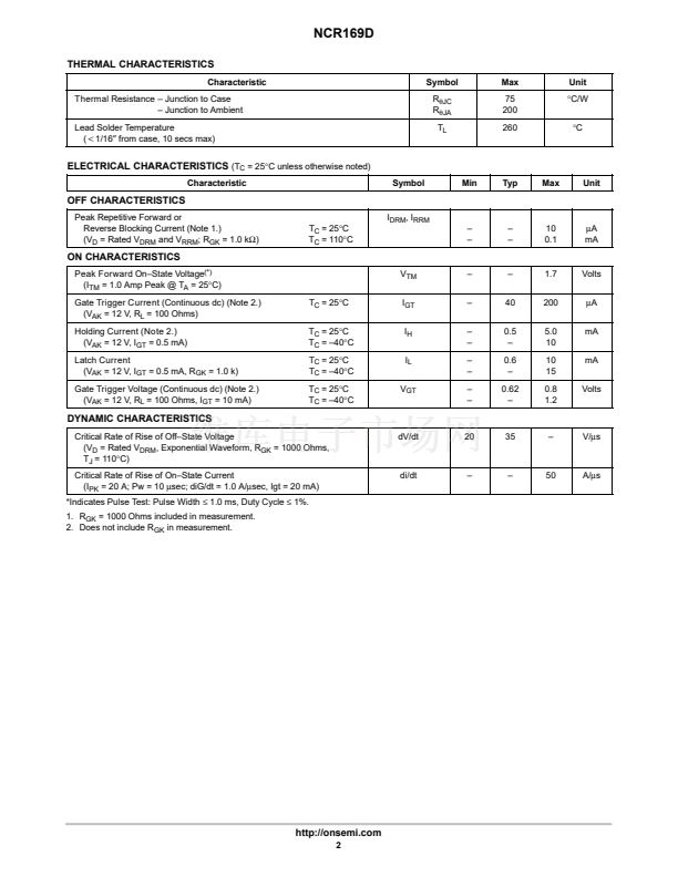
MAXIMUM RATINGS
(T
J
= 25擄C unless otherwise noted)
Rating
Peak Repetitive Off鈥揝tate Voltage (Note 1.)
(T
J
=
*40
to 110擄C, Sine Wave, 50 to
60 Hz; Gate Open)
On-State RMS Current
(T
C
= 80擄C) 180擄 Conduction Angles
Peak Non-Repetitive Surge Current
(1/2 Cycle, Sine Wave, 60 Hz,
T
J
= 25擄C)
Circuit Fusing Consideration (t = 10 ms)
Forward Peak Gate Power
(T
A
= 25擄C, Pulse Width
v
1.0
碌
s)
Forward Average Gate Power
(T
A
= 25擄C, t = 20 ms)
Forward Peak Gate Current
(T
A
= 25擄C, Pulse Width
v
1.0
碌
s)
Reverse Peak Gate Voltage
(T
A
= 25擄C, Pulse Width
v
1.0
碌
s)
Operating Junction Temperature Range
@ Rate V
RRM
and V
DRM
Storage Temperature Range
Symbol
V
DRM,
V
RRM
I
T(RMS)
I
TSM
Value
400
Unit
Volts
TO鈥?2
(TO鈥?26AA)
CASE 029
STYLE 10
K
G
http://onsemi.com
SCR
0.8 AMPERES RMS
400 VOLTS
G
A
K
MARKING
DIAGRAM
NCR
169D
YWW
0.8
10
Amp
Amps
A
Y
= Year
WW = Work Week
1 2 3
I
2
t
P
GM
P
G(AV)
I
GM
V
GRM
T
J
T
stg
0.415
0.1
0.10
1.0
5.0
鈥?0 to
110
鈥?0 to
150
A
2
s
Watt
PIN ASSIGNMENT
Watt
Amp
Volts
擄C
擄C
1
2
3
Cathode
Gate
Anode
ORDERING INFORMATION
See detailed ordering and shipping information in the package
dimensions section on page 6 of this data sheet.
1. V
DRM
and V
RRM
for all types can be applied on a continuous basis. Ratings
apply for zero or negative gate voltage; however, positive gate voltage shall
not be applied concurrent with negative potential on the anode. Blocking
voltages shall not be tested with a constant current source such that the
voltage ratings of the devices are exceeded.
This document contains information on a new product. Specifications and information
herein are subject to change without notice.
漏
Semiconductor Components Industries, LLC, 2000
1
December, 2000 鈥?Rev. 0
Publication Order Number:
NCR169D/D


 1
1
 2
2
 3
3
 4
4
 5
5
 6
6
 7
7
 8
8
