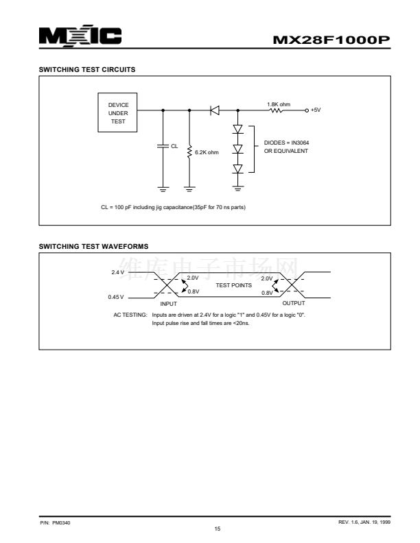
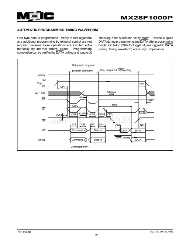
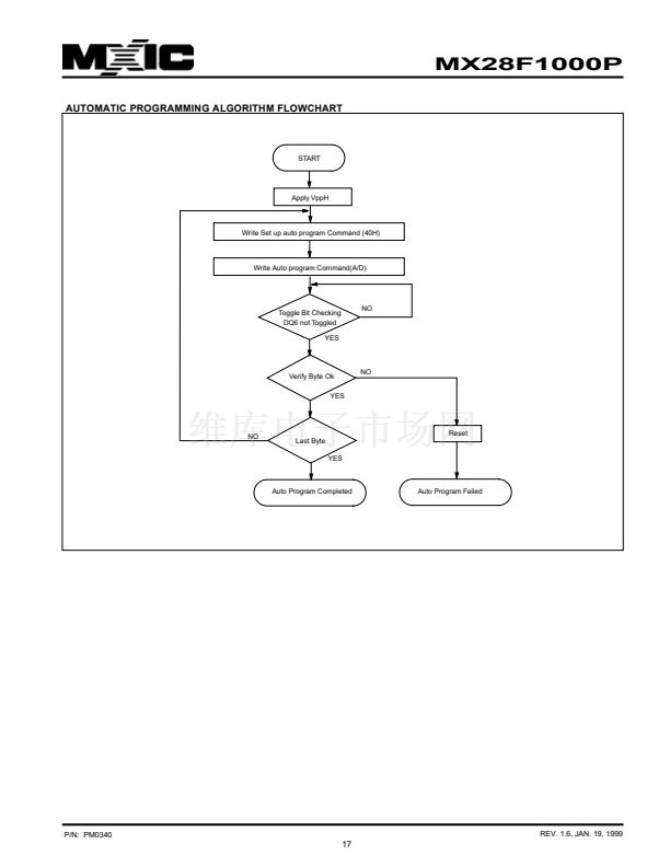
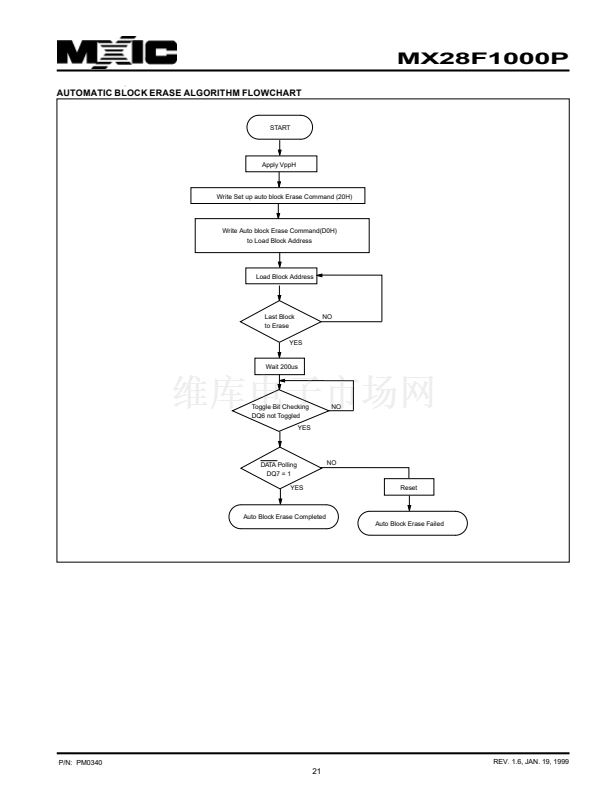
鈥?/div>
GENERAL DESCRIPTION
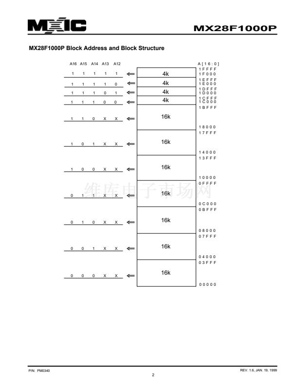
The MX28F1000P is a 1-mega bit Flash memory or-
ganized as 128K bytes of 8 bits each. MXIC's Flash
memories offer the most cost-effective and reliable
read/write non-volatile random access memory. The
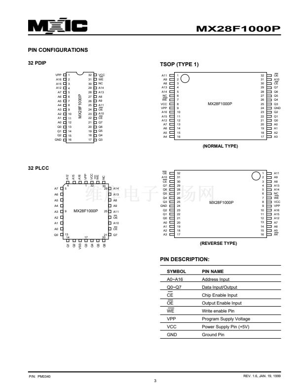
MX28F1000P is packaged in 32-pin PDIP, PLCC
and TSOP. It is designed to be reprogrammed and
erased in-system or in-standard EPROM program-
mers.
The standard MX28F1000P offers access times as
fast as 70 ns, allowing operation of high-speed
microprocessors without wait states. To eliminate
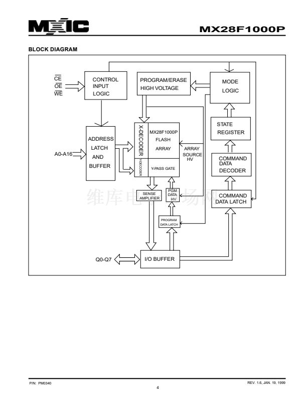
bus contention, the MX28F1000P has separate chip
enable (CE) and output enable (OE ) controls.
MXIC's Flash memories augment EPROM function-
ality with in-circuit electrical erasure and
programming. The MX28F1000P uses a command
register to manage this functionality, while
maintaining a standard 32-pin pinout. The
command register allows for 100% TTL level control
inputs and fixed power supply levels during erase
and programming, while maintaining maximum
EPROM compatibility.
MXIC Flash technology reliably stores memory con-
tents even after 10,000 erase and program cycles.
The MXIC cell is designed to optimize the erase and
programming mechanisms. In addition, the combi-
nation of advanced tunnel oxide processing and low
internal electric fields for erase and programming
operations produces reliable cycling.
The
MX28F1000P uses a 12.0V
鹵
5% VPP supply to
perform the Auto Program/Erase algorithms.
The highest degree of latch-up protection is
achieved with MXIC's proprietary non-epi process.
Latch-up protection is proved for stresses up to 100
milliamps on address and data pin from -1V to VCC
+ 1V.
P/N: PM0340
1
REV. 1.6,JAN. 19, 1999


 1
1
 2
2
 3
3
 4
4
 5
5
 6
6
 7
7
 8
8
 9
9
 10
10
 11
11
 12
12
 13
13
 14
14
 15
15
 16
16
 17
17
 18
18
 19
19
 20
20
 21
21
 22
22
 23
23
 24
24
 25
25
 26
26
 27
27
 28
28
 29
29
 30
30
 31
31
 32
32
 33
33
