MwT-0206S-2P2/0206Z-2P2
2.0-6.0 GHz Balanced Amplifier Module
www.mwtinc.com
Email: info@mwtinc.com
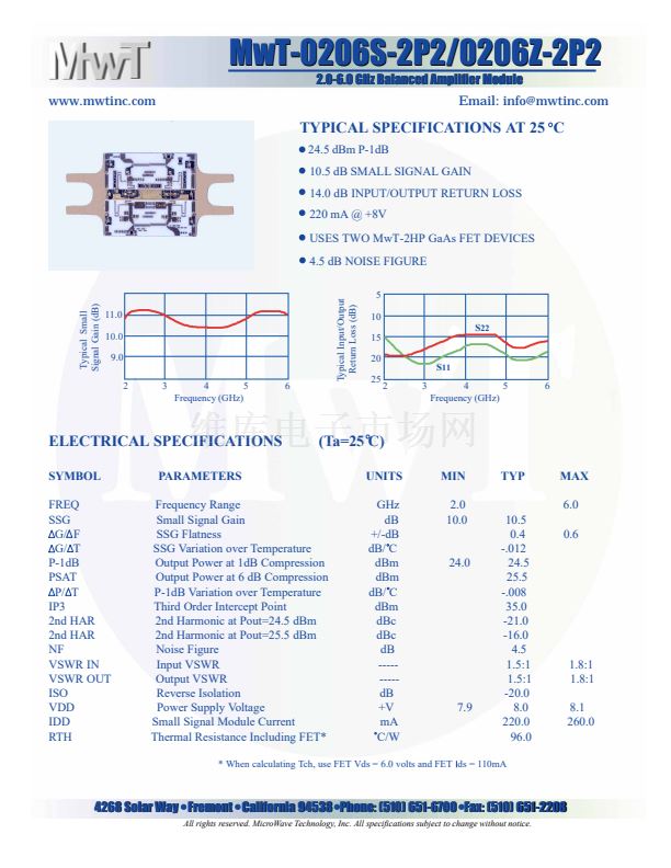
TYPICAL SPECIFICATIONS AT 25 C
24.5 dBm P-1dB
10.5 dB SMALL SIGNAL GAIN
14.0 dB INPUT/OUTPUT RETURN LOSS
220 mA @ +8V
USES TWO MwT-2HP GaAs FET DEVICES
4.5 dB NOISE FIGURE
5
10
S
22
15
20
25
2
3
S
11
4
5
Frequency (GHz)
6
11.0
10.0
9.0
2
3
4
5
Frequency (GHz)
6
ELECTRICAL SPECIFICATIONS
SYMBOL
FREQ
SSG
G/ F
G/ T
P-1dB
PSAT
P/ T
IP3
2nd HAR
2nd HAR
NF
VSWR IN
VSWR OUT
ISO
VDD
IDD
RTH
PARAMETERS
(Ta=25 C)
UNITS
GHz
dB
+/-dB
dB/ C
dBm
dBm
dB/ C
dBm
dBc
dBc
dB
-----
-----
dB
+V
mA
C/W
MIN
2.0
10.0
TYP
MAX
6.0
10.5
0.4
-.012
24.5
25.5
-.008
35.0
-21.0
-16.0
4.5
1.5:1
1.5:1
-20.0
8.0
220.0
96.0
0.6
Frequency Range
Small Signal Gain
SSG Flatness
SSG Variation over Temperature
Output Power at 1dB Compression
Output Power at 6 dB Compression
P-1dB Variation over Temperature
Third Order Intercept Point
2nd Harmonic at Pout=24.5 dBm
2nd Harmonic at Pout=25.5 dBm
Noise Figure
Input VSWR
Output VSWR
Reverse Isolation
Power Supply Voltage
Small Signal Module Current
Thermal Resistance Including FET*
Typical Input/Output
Return Loss (dB)
Typical Small
Signal Gain (dB)
24.0
1.8:1
1.8:1
8.1
260.0
7.9
* When calculating Tch, use FET Vds = 6.0 volts and FET ds = 110mA
4268 Solar Way Fremont California 94538 Phone: (510) 651-6700 Fax: (510) 651-2208
651-2208
All rights reserved. MicroWave Technology, Inc. All specifications subject to change without notice.


 1
1
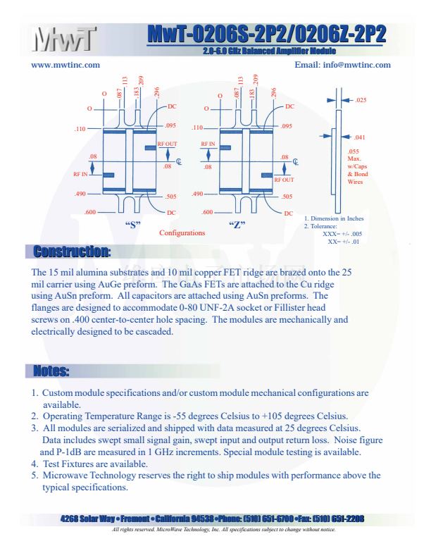 2
2
