MM54HC194 MM74HC194 4-Bit Bidirectional Universal Shift Register
November 1995
MM54HC194 MM74HC194
4-Bit Bidirectional Universal Shift Register
General Description
This 4-bit high speed bidirectional shift register utilizes ad-
vanced silicon-gate CMOS technology to achieve the low
power consumption and high noise immunity of standard
CMOS integrated circuits along with the ability to drive 10
LS-TTL loads This device operates at speeds similar to the
equivalent low power Schottky part
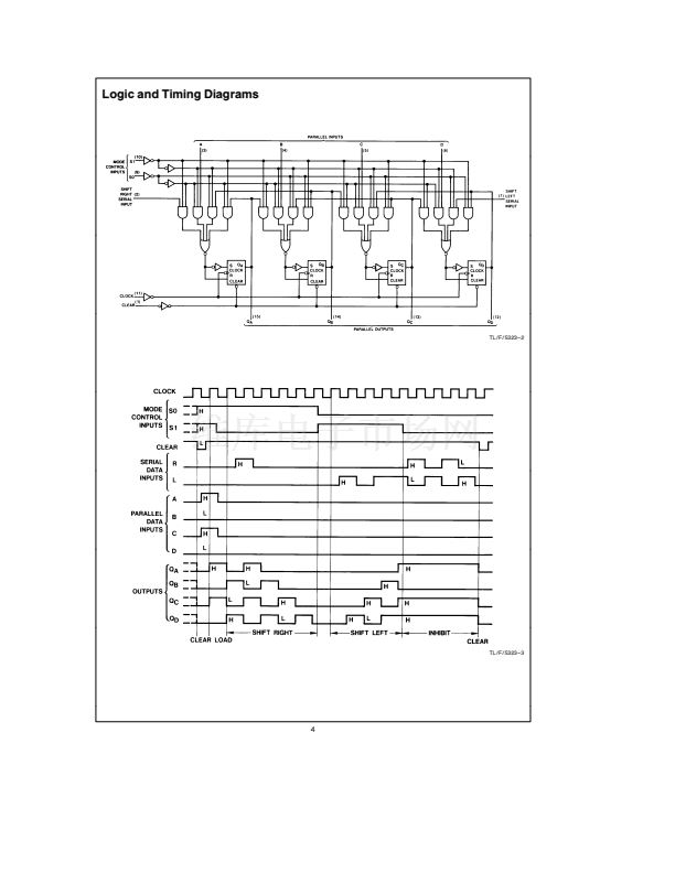
This bidirectional shift register is designed to incorporate
virtually all of the features a system designer may want in a
shift register It features parallel inputs parallel outputs
right shift and left shift serial inputs operating mode control
inputs and a direct overriding clear line The register has
four distinct modes of operation PARALLEL (broadside)
LOAD SHIFT RIGHT (in the direction Q
A
toward Q
D
)
SHIFT LEFT INHIBIT CLOCK (do nothing)
Synchronous parallel loading is accomplished by applying
the four bits of data and taking both mode control inputs S0
and S1 high The data are loaded into their respective flip
flops and appear at the outputs after the positive transition
of the CLOCK input During loading serial data flow is inhib-
ited Shift right is accomplished synchronously with the ris-
ing edge of the clock pulse when S0 is high and S1 is low
Serial data for this mode is entered at the SHIFT RIGHT
data input When S0 is low and S1 is high data shifts left
synchronously and new data is entered at the SHIFT LEFT
serial input Clocking of the flip flops is inhibited when both
mode control inputs are low The mode control inputs
should be changed only when the CLOCK input is high
The 54HC 74HC logic family is functionally as well as pin-
out compatible with the standard 54LS 74LS logic family
All inputs are protected from damage due to static dis-
charge by internal diode clamps to V
CC
and ground
Features
Y
Y
Y
Y
Y
Y
Typical operating frequency 45 MHz
Typical propagation delay ns (clock to Q)
Wide operating supply voltage range 2 鈥?6V
Low input current 1
mA
maximum
Low quiescent supply current 160
mA
maximum
(74HC Series)
Fanout of 10 LS-TTL loads
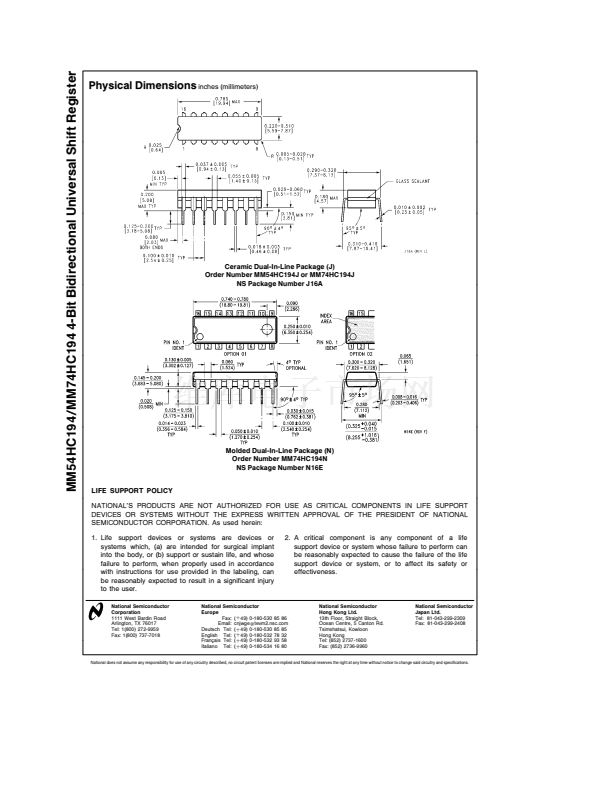
Connection Diagram
Dual-In Line Package
TL F 5323 鈥?1
Function Table
Inputs
Mode
Clear
L
H
H
H
H
H
H
H
S1 S2
X X
X X
H H
L H
L H
H L
H L
L L
Clock
X
L
Serial
X
X
X
X
X
H
L
X
X
X
X
H
L
X
X
X
Parallel
Q
A
Q
B
Q
C
Q
D
L
Q
A0
a
H
L
Q
Bn
Q
Bn
Q
A0
L
Q
B0
b
Q
An
Q
An
Q
Cn
Q
Cn
Q
B0
L
Q
C0
c
Q
Bn
Q
Bn
Q
Dn
Q
Dn
Q
C0
L
Q
D0
d
Q
Cn
Q
Cn
H
L
Q
D0
X
X
a
X
X
X
X
X
X
X
b
X
X
X
X
X
X
X
c
X
X
X
X
X
X
X
d
X
X
X
X
X
Left Right A B C D
Outputs
Order Number MM54HC194 or MM74HC194
H
e
high level (steady state)
L
e
low level (steady state)
X
e
irrelevant (any input including transitions)
u
e
transition from low to high level
a b c d
e
the level of steady-state input at inputs A B C or D
respectively
Q
A0
Q
B0
Q
C0
Q
D0
e
the level of Q
A
Q
B
Q
C
or Q
D
respectively
before the indicated steady-state input conditions were established
Q
An
Q
Bn
Q
Cn
Q
Dn
e
the level of Q
A
Q
B
Q
C
respectively before
transition of the clock
the most-recent
u
u
u
u
u
X
u
C
1995 National Semiconductor Corporation
TL F 5323
RRD-B30M115 Printed in U S A


 1
1
 2
2
 3
3
 4
4
 5
5
 6
6
