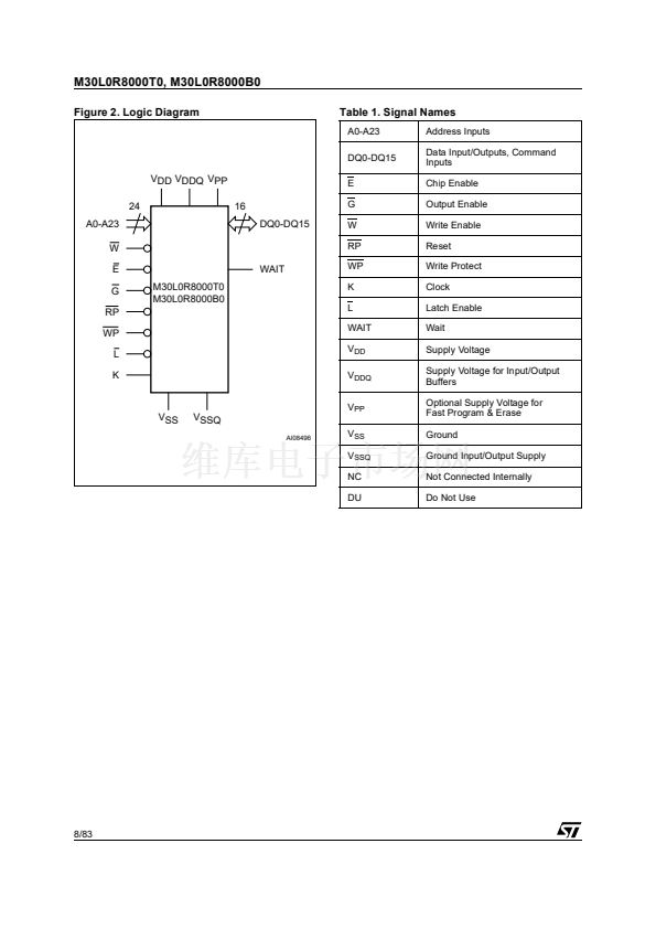
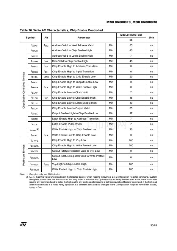
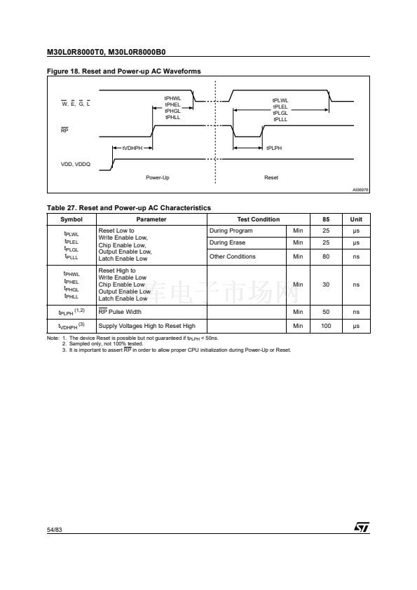
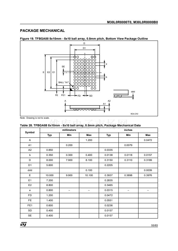
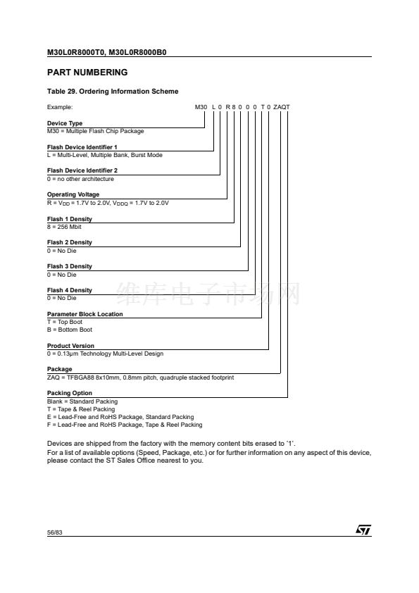
鈻?/div>
SUPPLY VOLTAGE
鈥?V
DD
= 1.7V to 2.0V for program, erase and
read
鈥?V
DDQ
= 1.7V to 2.0V for I/O Buffers
鈥?V
PP
= 9V for fast program (12V tolerant)
SYNCHRONOUS / ASYNCHRONOUS READ
鈥?Synchronous Burst Read mode:
54MHz
鈥?Asynchronous Page Read mode
鈥?Random Access: 85ns
SYNCHRONOUS BURST READ SUSPEND
PROGRAMMING TIME
鈥?10碌s typical Word program time using
Buffer Enhanced Factory Program
command
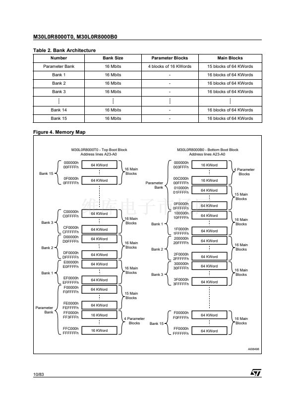
MEMORY ORGANIZATION
鈥?Multiple Bank Memory Array: 16 Mbit
Banks
鈥?Parameter Blocks (Top or Bottom
location)
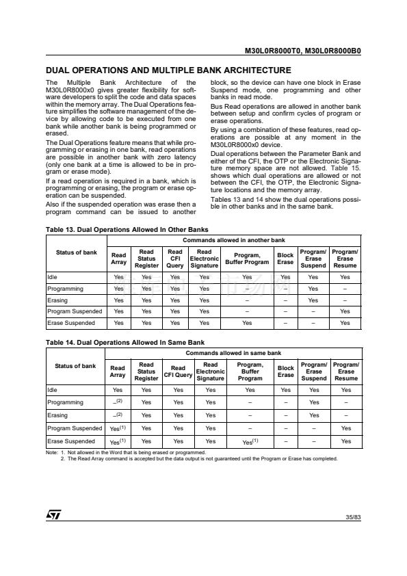
DUAL OPERATIONS
鈥?program/erase in one Bank while read in
others
鈥?No delay between read and write
operations
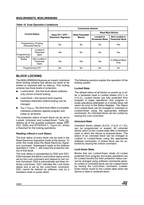
BLOCK LOCKING
鈥?All blocks locked at power-up
鈥?Any combination of blocks can be locked
with zero latency
鈥?WP for Block Lock-Down
鈥?Absolute Write Protection with V
PP
= V
SS
SECURITY
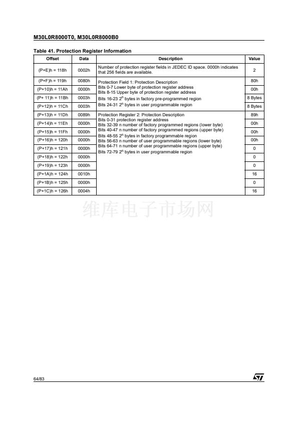
鈥?64 bit unique device number
鈥?2112 bit user programmable OTP Cells
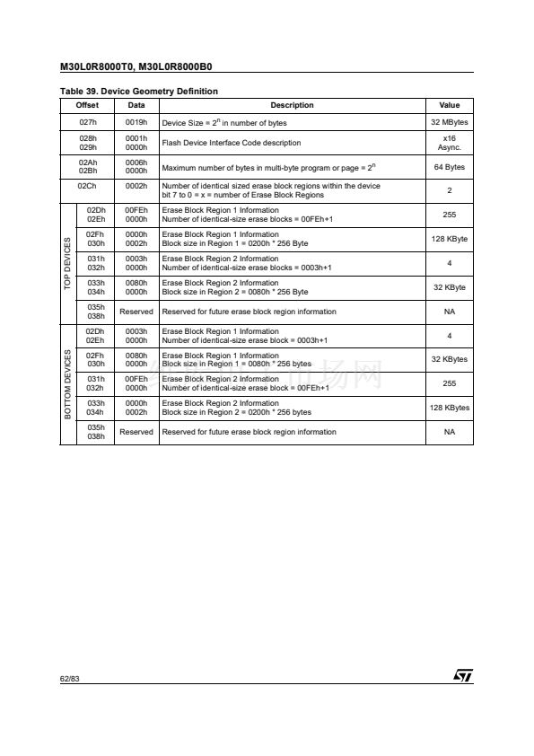
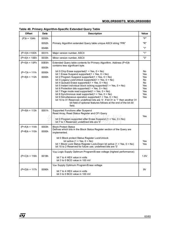
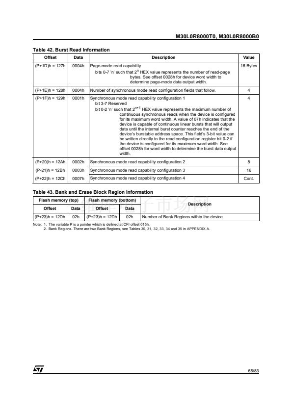
COMMON FLASH INTERFACE (CFI)
100,000 PROGRAM/ERASE CYCLES per
BLOCK
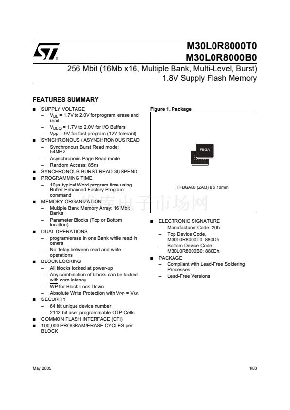
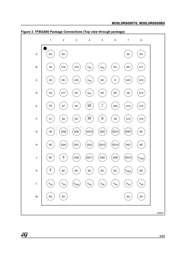
Figure 1. Package
FBGA
TFBGA88 (ZAQ) 8 x 10mm
鈻?/div>
鈻?/div>
ELECTRONIC SIGNATURE
鈥?Manufacturer Code: 20h
鈥?Top Device Code,
M30L0R8000T0: 880Dh.
鈥?Bottom Device Code,
M30L0R8000B0: 880Eh.
PACKAGE
鈥?Compliant with Lead-Free Soldering
Processes
鈥?Lead-Free Versions
May 2005
1/83


 1
1
 2
2
 3
3
 4
4
 5
5
 6
6
 7
7
 8
8
 9
9
 10
10
 11
11
 12
12
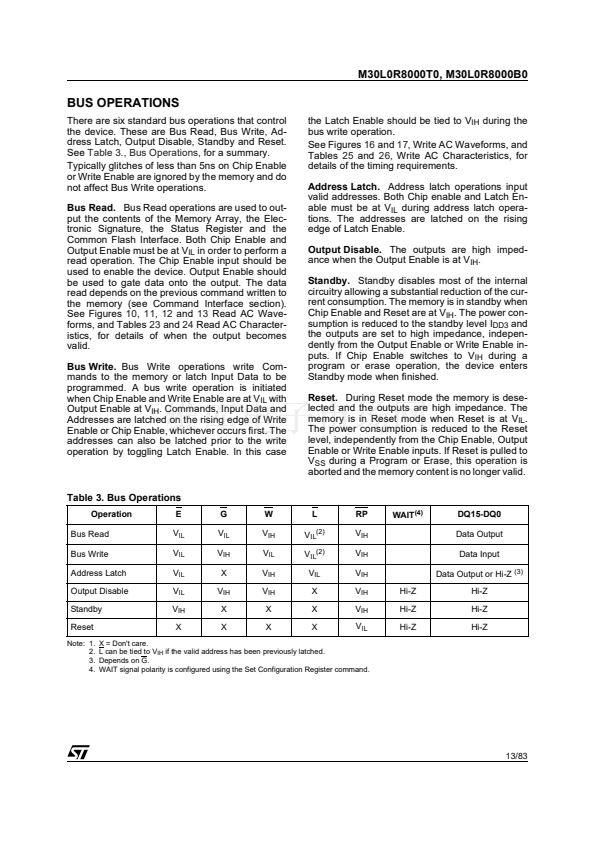 13
13
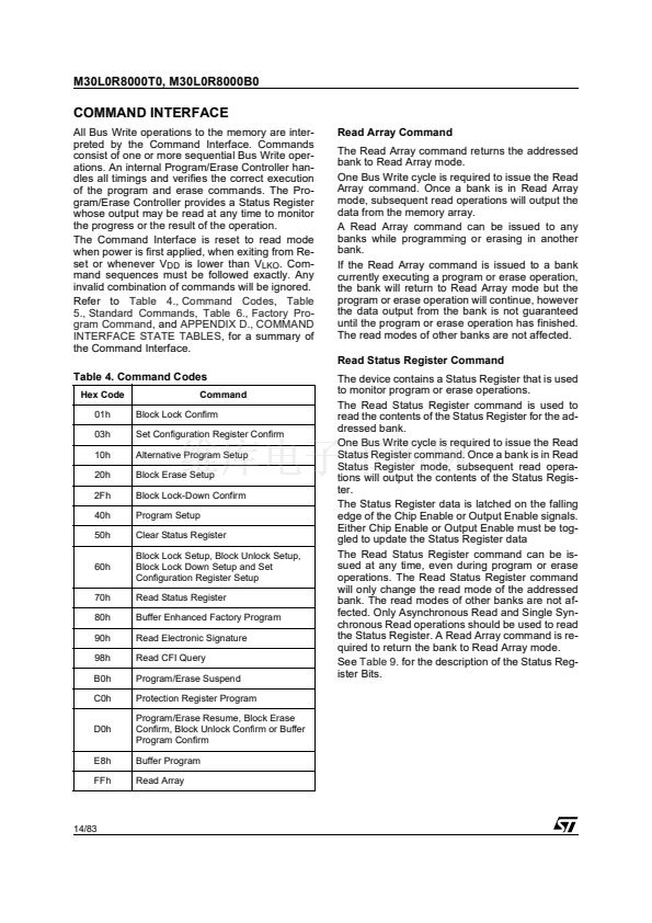 14
14
 15
15
 16
16
 17
17
 18
18
 19
19
 20
20
 21
21
 22
22
 23
23
 24
24
 25
25
 26
26
 27
27
 28
28
 29
29
 30
30
 31
31
 32
32
 33
33
 34
34
 35
35
 36
36
 37
37
 38
38
 39
39
 40
40
 41
41
 42
42
 43
43
 44
44
 45
45
 46
46
 47
47
 48
48
 49
49
 50
50
 51
51
 52
52
 53
53
 54
54
 55
55
 56
56
 57
57
 58
58
 59
59
 60
60
 61
61
 62
62
 63
63
 64
64
 65
65
 66
66
 67
67
 68
68
 69
69
 70
70
 71
71
 72
72
 73
73
 74
74
 75
75
 76
76
 77
77
 78
78
 79
79
 80
80
 81
81
 82
82
 83
83
