M29W008AT
M29W008AB
8 Mbit (1Mb x8, Boot Block)
Low Voltage Single Supply Flash Memory
s
2.7V to 3.6V SUPPLY VOLTAGE for
PROGRAM, ERASE and READ OPERATIONS
ACCESS TIME: 80ns
PROGRAMMING TIME: 10碌s typical
PROGRAM/ERASE CONTROLLER (P/E.C.)
鈥?Program Byte-by-Byte
鈥?Status Register bits and Ready/Busy Output
s
s
s
s
s
s
SECURITY PROTECTION MEMORY AREA
INSTRUCTIONS ADDRESS CODING: 3 digits
MEMORY BLOCKS
鈥?Boot Block (Top or Bottom location)
鈥?Parameter and Main blocks
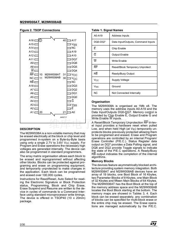
TSOP40 (N)
10 x 20mm
s
s
BLOCK, MULTI-BLOCK and CHIP ERASE
MULTI BLOCK PROTECTION/TEMPORARY
UNPROTECTION MODES
ERASE SUSPEND and RESUME MODES
鈥?Read and Program another Block during
Erase Suspend
Figure 1. Logic Diagram
s
s
LOW POWER CONSUMPTION
鈥?Stand-by and Automatic Stand-by
100,000 PROGRAM/ERASE CYCLES per
BLOCK
20 YEARS DATA RETENTION
鈥?Defectivity below 1ppm/year
ELECTRONIC SIGNATURE
鈥?Manufacturer Code: 20h
鈥?Top Device Code, M29W008AT: D2h
鈥?Bottom Device Code, M29W008AB: DCh
G
RP
VCC
s
20
A0-A19
W
E
M29W008AT
M29W008AB
8
DQ0-DQ7
s
s
RB
VSS
AI02716
March 2000
1/30


 1
1
 2
2
 3
3
 4
4
 5
5
 6
6
 7
7
 8
8
 9
9
 10
10
 11
11
 12
12
 13
13
 14
14
 15
15
 16
16
 17
17
 18
18
 19
19
 20
20
 21
21
 22
22
 23
23
 24
24
 25
25
 26
26
 27
27
 28
28
 29
29
 30
30
