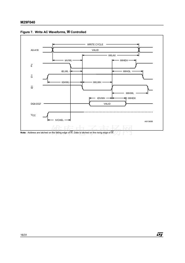
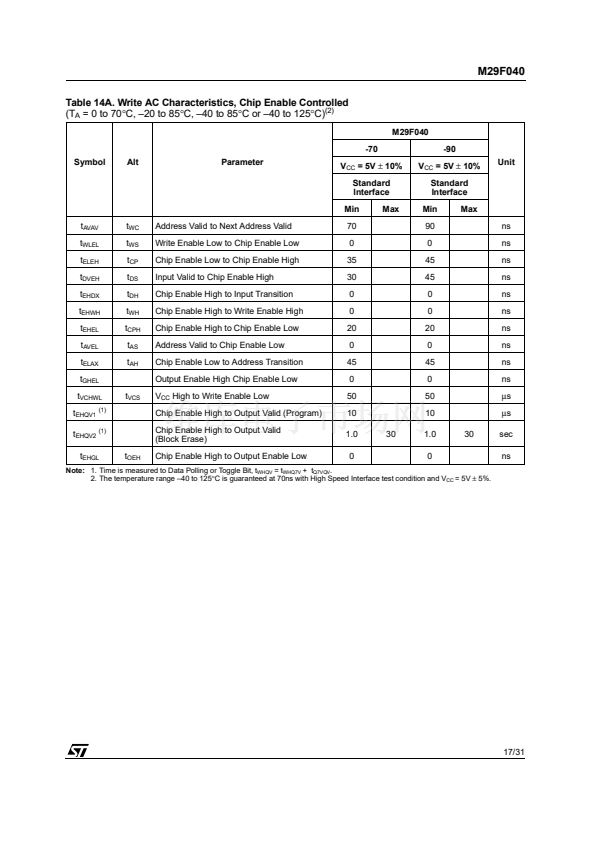
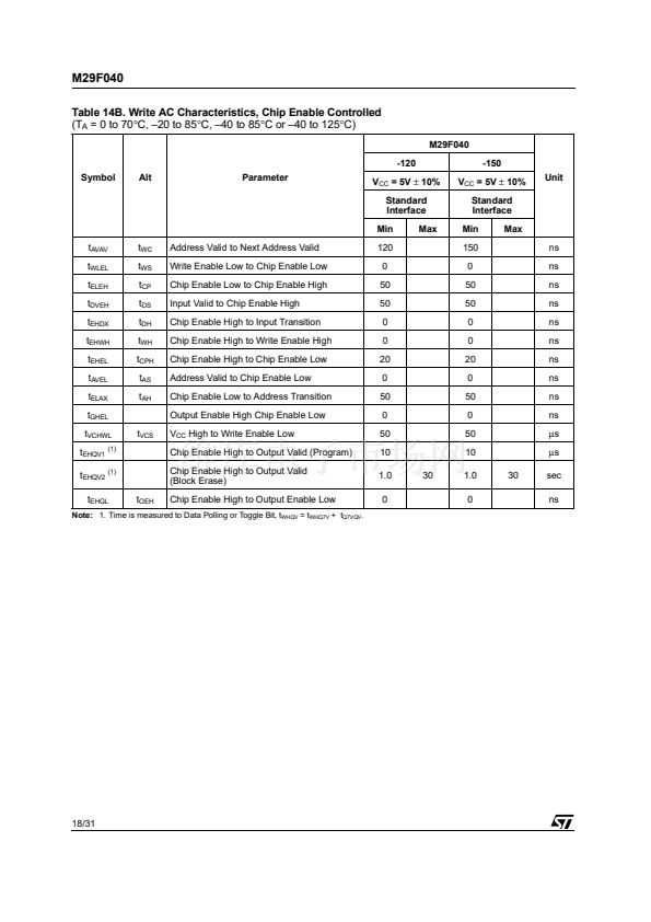
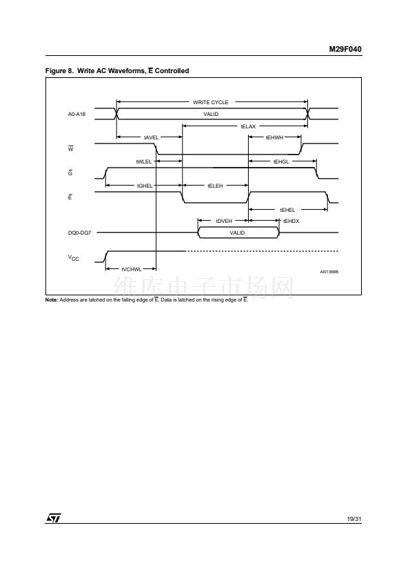
M29F040
4 Mbit (512Kb x8, Uniform Block) Single Supply Flash Memory
NOT FOR NEW DESIGN
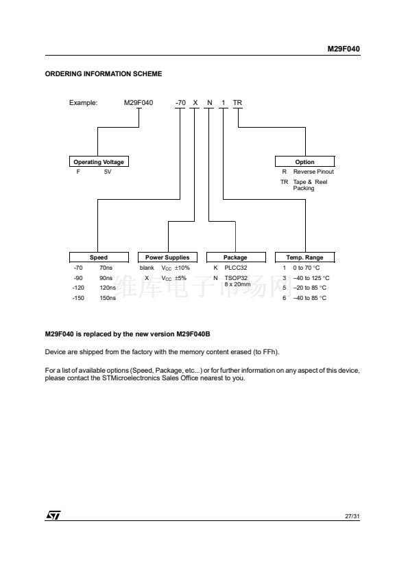
M29F040 is replaced by the M29F040B
5V
鹵
10% SUPPLY VOLTAGE for PROGRAM,
ERASE and READ OPERATIONS
FAST ACCESS TIME: 70ns
BYTE PROGRAMMING TIME: 10碌s typical
ERASE TIME
鈥?Block: 1.0 sec typical
鈥?Chip: 2.5 sec typical
PROGRAM/ERASE CONTROLLER (P/E.C.)
鈥?Program Byte-by-Byte
鈥?Data Polling and Toggle bits Protocol for
P/E.C. Status
MEMORY ERASE in BLOCKS
鈥?8 Uniform Blocks of 64 KBytes each
鈥?Block Protection
鈥?Multiblock Erase
ERASE SUSPEND and RESUME MODES
LOW POWER CONSUMPTION
鈥?Read mode: 8mA typical (at 12MHz)
鈥?Stand-by mode: 25碌A(chǔ) typical
鈥?Automatic Stand-by mode
100,000 PROGRAM/ERASE CYCLES per
BLOCK
20 YEARS DATA RETENTION
鈥?Defectivity below 1ppm/year
ELECTRONIC SIGNATURE
鈥?Manufacturer Code: 20h
鈥?Device Code: E2h
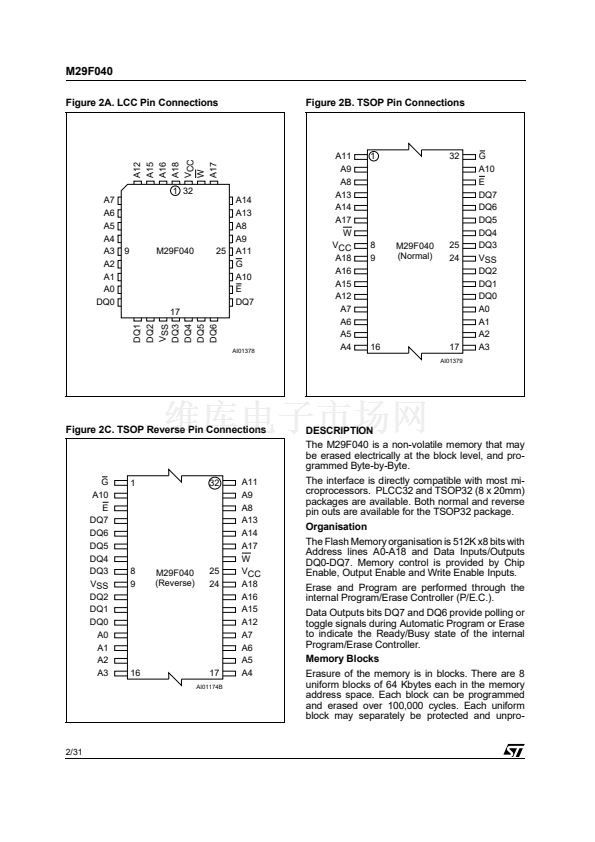
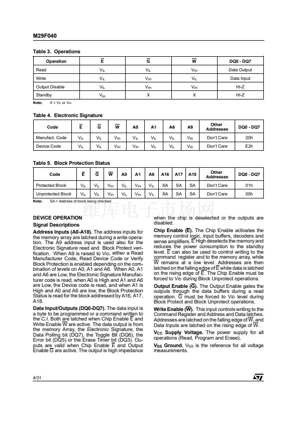
Table 1. Signal Names
A0-A18
DQ0-DQ7
E
G
W
V
CC
V
SS
Address Inputs
Data Input / Outputs
Chip Enable
Output Enable
Write Enable
Supply Voltage
Ground
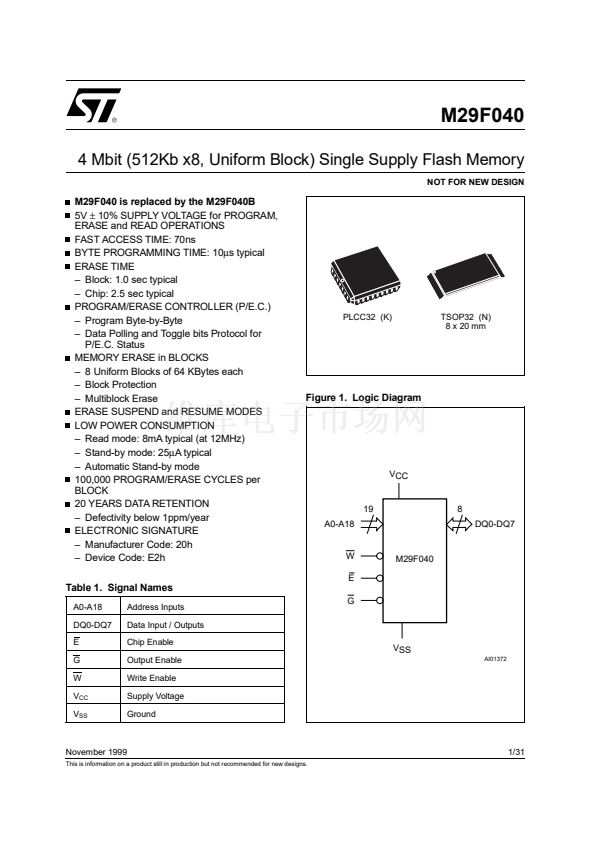
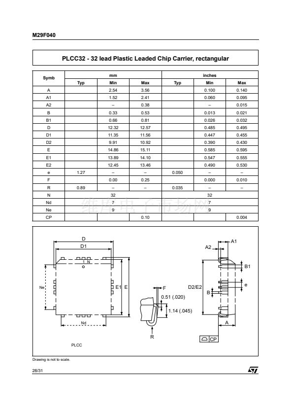
PLCC32 (K)
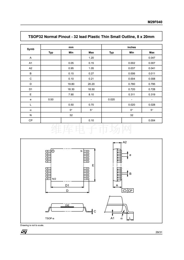
TSOP32 (N)
8 x 20 mm
Figure 1. Logic Diagram
VCC
19
A0-A18
8
DQ0-DQ7
W
E
G
M29F040
VSS
AI01372
November 1999
This is information on a product still in production but not recommended for new designs.
1/31


 1
1
 2
2
 3
3
 4
4
 5
5
 6
6
 7
7
 8
8
 9
9
 10
10
 11
11
 12
12
 13
13
 14
14
 15
15
 16
16
 17
17
 18
18
 19
19
 20
20
 21
21
 22
22
 23
23
 24
24
 25
25
 26
26
 27
27
 28
28
 29
29
 30
30
 31
31
