LM9630 100 x 128, 580 fps Ultra Sensitive Monochrome CMOS Image Sensor
ADVANCE INFORMATION
May 2002
LM9630 100 x 128, 580 fps Ultra Sensitive Monochrome CMOS Image Sensor
General Description
The LM9630 is a high performance, low power, CMOS Active
Pixel Image Sensor capable of capturing monochrome images
at 580 frames per second.
In addition to the active pixel array, an on-chip 8 bit A/D conver-
tor, fixed pattern noise elimination circuits a d a video gain
n
amplifier are provided.
The integrated programmable timing and control circuit allows
the user maximum flexibility in adjusting integration time and
frame rate. Furthermore, a fast read out circuit is provided allow-
ing a full frame to read out on a single 8-bit digital data bus in
less than 2ms.
The sensor utilizes a patented pixel design that incorporates an
integrated electronic shutter. This together with its ultra high sen-
sitivity makes the LM9630 an ideal choice for low light imaging
applications or applications where images of fast moving objects
need to be captured with minimum motion blur.
Key Specifications
Array Format
Total
Active
Effective Image Area
Total
Active
Optical Format
Pixel Size
Video Outputs
Frame Rate
Dynamic Range
Electronic Shutter
FPN
128H x 101V
118H x 96V
2.56 mm x 2.00 mm
2.36 mm x 1.92 mm
1/5鈥?/div>
20碌m x 20碌m
8 Bit Digital
580 frames per second
48 dB
Global Reset
0.5%
1.3%
22 Volt/lux.s
47%
32 CLCC
3.3V +/- 10%
110 mW
-40
o
C to 85
o
C
Applications
f
f
f
High Speed Motion Detection
IR Imaging
Low Light Imaging Applications
PRMU
Sensitivity
Fill Factor
Package
Features
f
f
f
f
f
f
f
f
f
f
f
Electronic shutter with global reset & pixel exposure.
Programmable analog video gain.
Integrated 8 bit analog to digital conversion.
Programmable integration time.
Programmable frame rate.
Master and slave mode of operation
On chip black level compensation.
Power down and low power modes.
I
2
C compatible serial interface.
10 bit digital video port (8 data, vertical & horizontal sync).
Power on reset with hardware and software override.
Single Supply
Power Consumption
Operating Temp
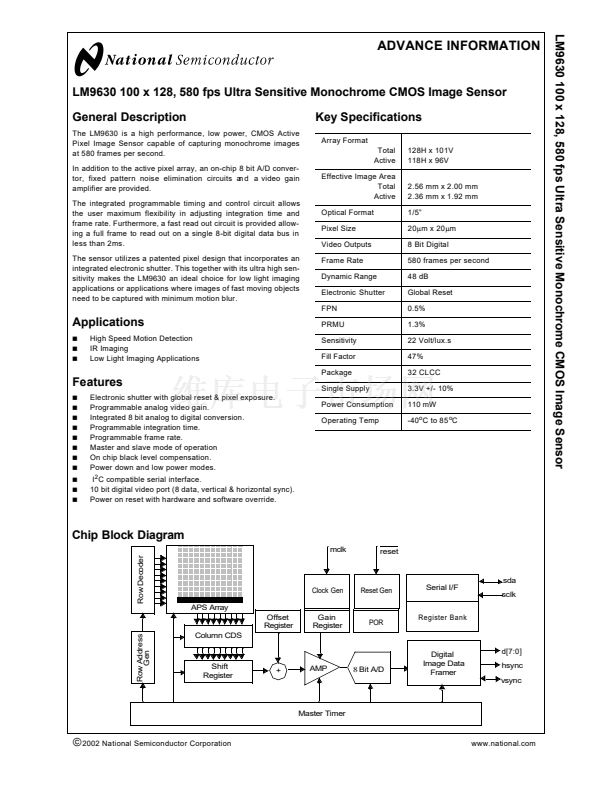
Chip Block Diagram
mclk
Row Decoder
reset
sda
Clock Gen
APS Array
Offset
Register
Gain
Register
POR
Register Bank
Reset Gen
Serial I/F
sclk
Row Address
Gen
Column CDS
Digital
Image Data
Framer
d[7:0]
hsync
vsync
Shift
Register
+
AMP
8
Bit A/D
Master Timer
漏
2002 National Semiconductor Corporation
www.national.com


 1
1
 2
2
