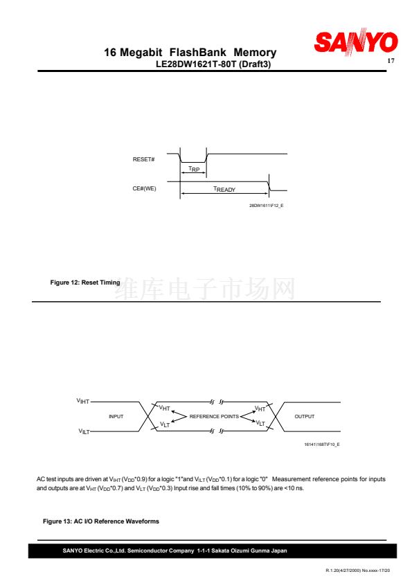
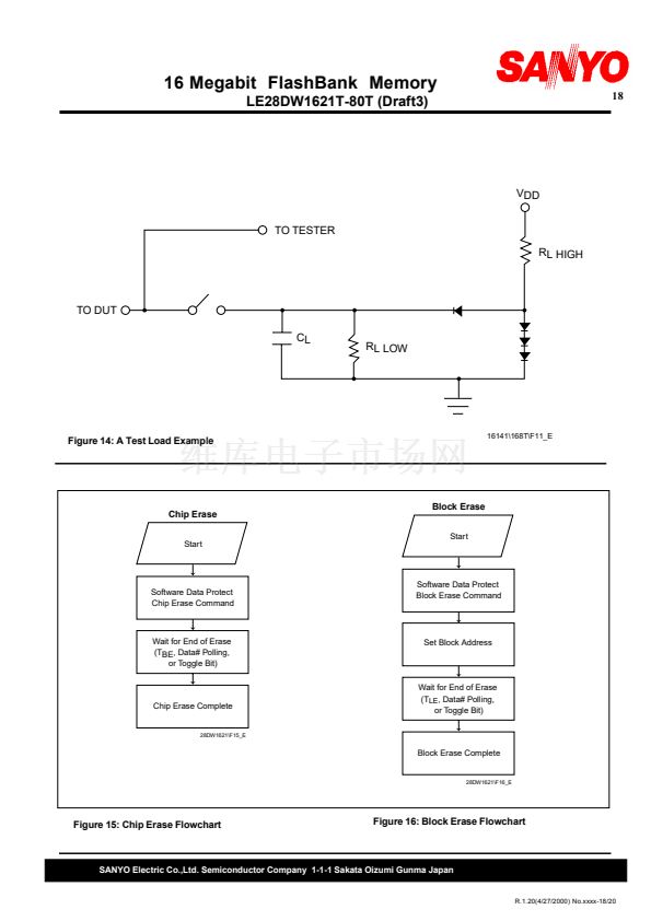
鈥?/div>
Fixed Erase, Program, Write Times
鈥?Does not change after cycling
Product Description
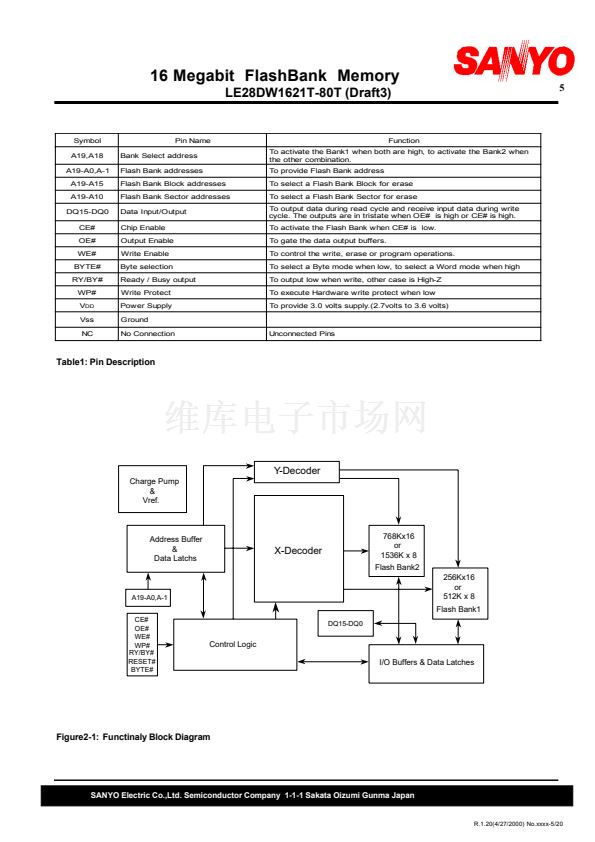
The LE28DW1621T consists of two memory banks, Bank1 is
a 256K x 16 bits or 512K x 8 sector mode flash EEPROM and
Bank2 is a 768K x 16 bits or 1536K x 8 sector mode flash
EEPROM, manufactured with SANYO's proprietary, high per-
formance FlashTechnology. The LE28DW1621T writes with a
3.0-volt-only power supply.
The LE28DW1621T is divided into two separate memory banks.
Bank1 contains 256 sectors of 1K words or 8 blocks of 32K
words, Bank2 contains 768 sectors of 1K words or 24 blocks of
32K words.
Any bank may be used for executing code while writing data to
a different bank. Each memory bank is controlled by separate
Bank selection address (A18,A19) lines.
The LE28DW1621T inherently uses less energy during Erase,
and Program than alternative flash technologies. The total
energy consumed is a function of the applied voltage, current,
and time of application. Since for any given voltage range, the
Flash technology uses less current to program and has a shorter
Erase time, the total energy consumed during any Erase or
Program operation is less than alternative flash technologies.
The Auto Low Power mode automatically reduces the active
read current to approximately the same as standby; thus,
providing an average read current of approximately 1 mA/MHz of
Read cycle time.
The Flash technology provides fixed Erase and Program times,
independent of the number of erase/program cycles that have
occurred. Therefore the system software or hardware does not
Pr
el
im
in
ar
y
have to be modified or derated as is necessary with alternative
flash technologies, whose Erase and Program times increase
with accumulated erase/program cycles.
Device Operation
The LE28DW1621T operates as independent 4Megabit and
12Megabit Word Pogram, Sector Erase flash EEPROMs. Two
memory Banks are spareted by the address space.
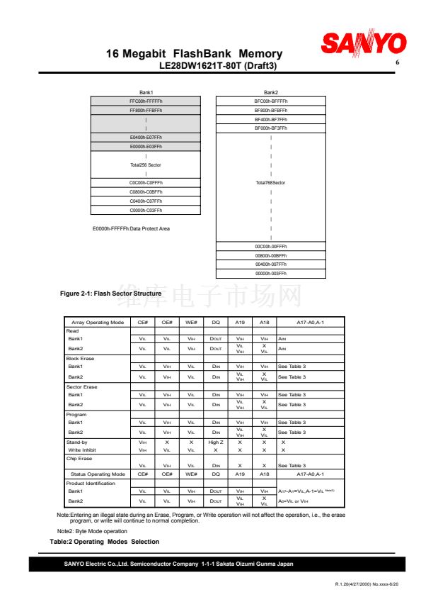
The Bank1 is assigned as C0000h to FFFFFh, Bank2 is as-
signed as 00000h to BFFFFh.
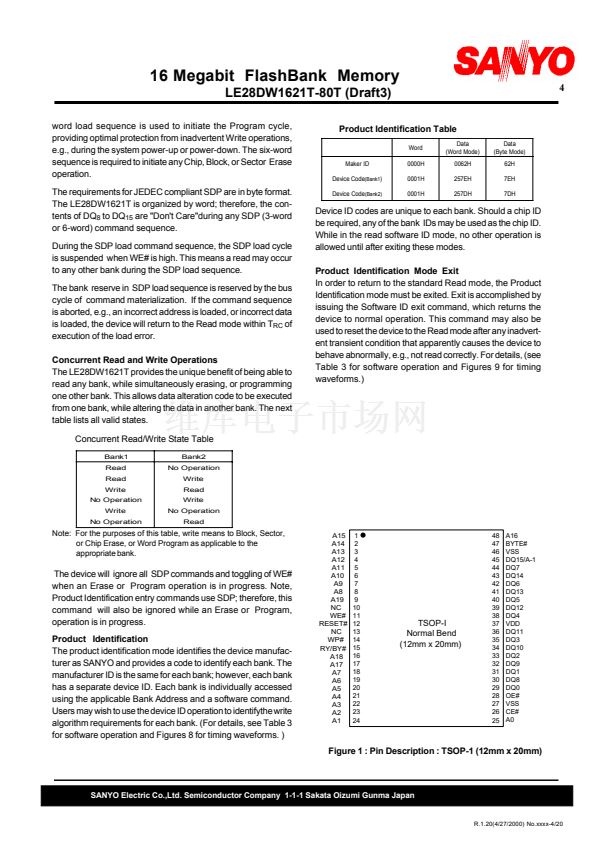
All memory banks share common I/O lines, WE#, and OE#.
Memory bank selection is by bank select address(A19, A18).
WE# is used with SDP to control the Erase and Program
operation in each memory bank.
The LE28DW1621T provides the added functionality of being
able to simultaneously read from one memory bank while
erasing, or programming to one other memory bank. Once the
internally controlled Erase or Program cycle in a memory bank
has commenced, a different memory bank can be accessed for
read. Also, once WE# and CE# are high during the SDP load
sequence, a different bank may be accessed to read.
LE28DW1621T which selectes banks (A19, A18) by a address.
It can be used as a normal conventinal flash memory when
operats erase or program operation to only a bank at non-
concurrent operation.
The device ID cannot be accessed while any bank is writing,
erasing, or programming.
SANYO Electric Co.,Ltd. Semiconductor Company 1-1-1
1
Sakata Oizumi Gunma Japan
The Flash Bank product family was jointly developed by SANYO and Sillicon Storage Technology,Inc.(SST),under SST's technology license. This preliminary specification is subject to change
without notice.
R.1.20(4/27/2000) No.xxxx-1/20


 1
1
 2
2
 3
3
 4
4
 5
5
 6
6
 7
7
 8
8
 9
9
 10
10
 11
11
 12
12
 13
13
 14
14
 15
15
 16
16
 17
17
 18
18
 19
19
 20
20
