KSK30
KSK30
Low Noise PRE-AMP. Use
鈥?High Input Impedance: I
GSS
=1nA (MAX)
鈥?Low Noise: NF=0.5dB (TYP)
鈥?High Voltage: V
GDS
= -50V
1
TO-92
1. Source 2. Gate 3. Drain
Silicon N-channel Junction Fet
Absolute Maximum Ratings
T
a
=25擄C unless otherwise noted
Symbol
V
GDS
I
G
P
D
T
J
T
STG
Gate-Drain Voltage
Gate-Current
Collector Dissipation
Junction Temperature
Storage Temperature
Parameter
Ratings
-50
10
100
125
-55 ~ 125
Units
V
mA
mW
擄C
擄C
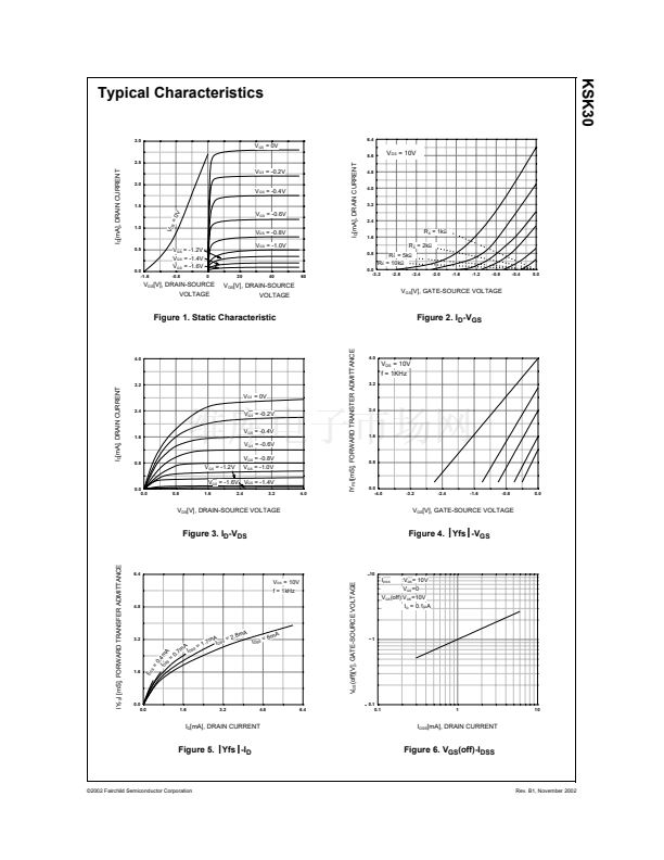
Electrical Characteristics
T
a
=25擄C unless otherwise noted
Symbol
BV
GDS
I
GSS
I
DSS
V
GS
(off)
錚
FS
錚?/div>
C
iss
C
rss
NF
Parameter
Gate-Drain Breakdown Voltage
Gate Leak Current
Drain Leak Current
Gate-Source Voltage
Forward Transfer Admittance
Input Capacitance
Feedback Capacitance
Noise Figure
Test Condition
V
DS
=0, I
G
= -100碌A(chǔ)
V
GS
= -30V, V
DS
=0
V
DS
=10V, V
GS
=0
V
DS
=10V, I
D
=0.1碌A(chǔ)
V
DS
=10V, V
GS
=0, f=1KHz
V
DS
=0, V
GS
=0, f=1MHz
V
GD
=10V, V
DS
=0
f=1MHz
V
DS
=15V, V
GS
=0
R
G
=100K鈩?/div>
f=120Hz
0.3
-0.4
1.2
8.2
2.6
0.5
5
Min.
-50
Typ.
Max.
-1
6.5
-5
Units
V
nA
mA
V
mS
pF
pF
dB
I
DSS
Classification
Classification
I
DSS
(mA)
R
0.30 ~ 0.75
O
0.60 ~ 1.40
Y
1.20 ~ 3.00
G
2.60 ~ 6.50
漏2002 Fairchild Semiconductor Corporation
Rev. B1, November 2002


 1
1
 2
2
 3
3
 4
4
 5
5
