TECHNICAL DATA
KK4541B
Programmable Timer
High-Performance Silicon-Gate CMOS
The KK4541B programmable timer consists of a 16-stage binary
counter, an oscillator that is controlled by external R-C components (2
resistors and a capacitor), an automatic power-on reset circuit, and output
control logic. The counter increments on positive-edge clock transitons
and can also be reset via the MASTER RESET input.
The output from this timer is the Q or not Q output from the 8th, 10th,
13th, or 16th counter stage. The desired stage is chosen using time-select
inputs A and B. The output is available in either of two modes selectable
via the MODE input, pin 10. When this MODE input is a logic 鈥?鈥?the
output will be a continuous square wave having a frequency equal to the
oscillator frequency divided by 2
N
. With the MODE input set to logic 鈥?鈥?/div>
ORDERING INFORMATION
and after a MASTER RESET is initiated, the output (assuming Q output
KK4541BN Plastic
N-1
has been selected) changes from a low to a high state after 2 counts and
KK4541BD SOIC
remains in that state until another MASTER RESET pulse is applied or
T
A
= -55擄 to 125擄 C for all packages
the MODE input is set to a logic 鈥?鈥?
Timing is initialized by setting the AUTO RESET input (pin 5) to
logic 鈥?鈥漚nd turning power on. If pin 5 is set to logic 鈥?鈥? the AUTO RESET circuit is disabled and counting will not
start untill after a positive MASTER RESET pulse is applied and returns to a low level. The AUTO RESET consumes
an appreciable amount of power and should not be used if low-power operation is desired. For reliable automatic
power-on reset, V
CC
should be greater than 5V.
鈥?/div>
Operating Voltage Range: 3.0 to 18 V
鈥?/div>
Maximum input current of 1
碌A(chǔ)
at 18 V over full package-temperature range; 100 nA at 18 V and 25擄C
鈥?/div>
Noise margin (over full package temperature range):
1.0 V min @ 5.0 V supply
2.0 V min @ 10.0 V supply
2.5 V min @ 15.0 V supply
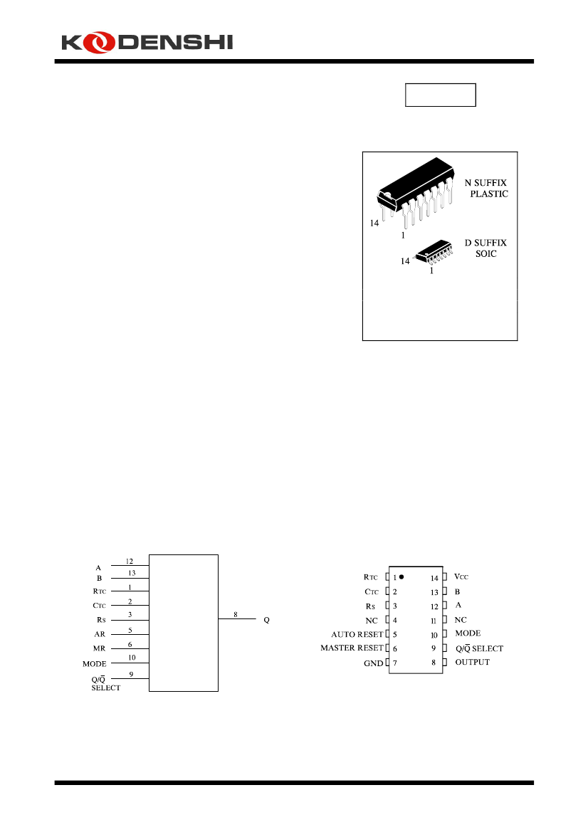
LOGIC DIAGRAM
PIN ASSIGNMENT
NC = NO CONNECTION
PIN 14 =V
CC
PIN 7 = GND
PINS 4,11 = NO CONNECTION
1


 1
1
 2
2
 3
3
 4
4
 5
5
 6
6
