K9F3208W0A-TCB0, K9F3208W0A-TIB0
Document Title
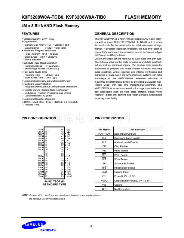
4M x 8 Bit NAND Flash Memory
FLASH MEMORY
Revision History
Revision No. History
0.0
0.1
Initial issue.
Data Sheet, 1999
1. Added CE don鈥檛 care mode during the data-loading and reading
0.2
1. Revised real-time map-out algorithm(refer to technical notes)
2. Removed erase suspend/resume mode
1. Changed device name
- KM29W32000AT -> K9F3208W0A-TCB0
- KM29W32000AIT -> K9F3208W0A-TIB0
1. Changed invalid block(s) marking method prior to shipping
- The invalid block(s) information is written the 1st or 2nd page of the
invalid block(s) with 00h data
--->The invalid block(s) status is defined by the 6th byte in the spare
area. Samsung makes sure that either the 1st or 2nd page of every
invalid block has
non-FFh
data at the column address of 517.
2. Changed SE pin description
- SE is recommended to coupled to GND or Vcc and should not be
toggled during reading or programming.
1.Powerup sequence is added
: Recovery time of minimum 1碌s is required before internal circuit gets
ready for any command sequences
~ 2.5V
Draft Date
April 10th 1998
April 10th 1999
Remark
Advance
July 23th 1999
0.3
Sep. 15th 1999
0.4
July 17th 2000
0.5
July 23th 2001
鈮?/div>
~ 2.5V
V
CC
High
WP
WE
2. AC parameter tCLR(CLE to RE Delay, min 50ns) is added.
3. AC parameter tAR1 value : 150ns --> 20ns
4. #40 Pin Name : nSE --> GND
Note : For more detailed features and specifications including FAQ, please refer to Samsung鈥檚 Flash web site.
http://www.intl.samsungsemi.com/Memory/Flash/datasheets.html.
The attached datasheets are prepared and approved by SAMSUNG Electronics. SAMSUNG Electronics CO., LTD. reserve the right
to change the specifications. SAMSUNG Electronics will evaluate and reply to your requests and questions about device. If you have
any questions, please contact the SAMSUNG branch office near you.


 1
1
 2
2
 3
3
 4
4
 5
5
 6
6
 7
7
 8
8
 9
9
 10
10
 11
11
 12
12
 13
13
 14
14
 15
15
 16
16
 17
17
 18
18
 19
19
 20
20
 21
21
 22
22
 23
23
 24
24
 25
25
 26
26
 27
27
