WRITE ALLBYTEs( K鈫?/div>
) :
from "H" to " L"
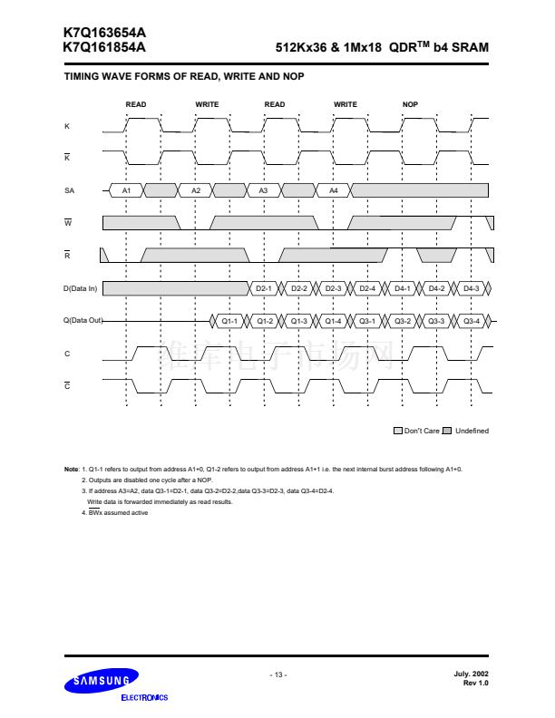
2) Page 13 TIMING WAVE FORMS Note 2 supplement
1. 1.8V I/O supply voltage addition
1) Page 2 FEATURES
2) Page 3,4 PIN NAME V
DDQ
3) Page 10, OPERATING CONTITIONS
4) Page 11 AC TEST CONTITIONS
2. Amendment
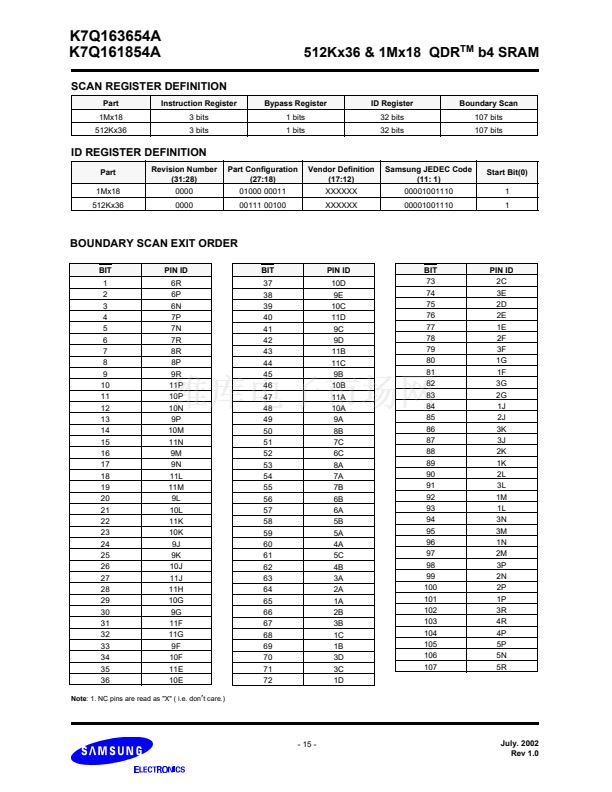
1) Page 15 BOUNDARY SCAN ORDER EXIT
1. Icc, Isb addition
2. 1.8V Vddq addition
1. Reserved pin for high density name change from NC to Vss/SA
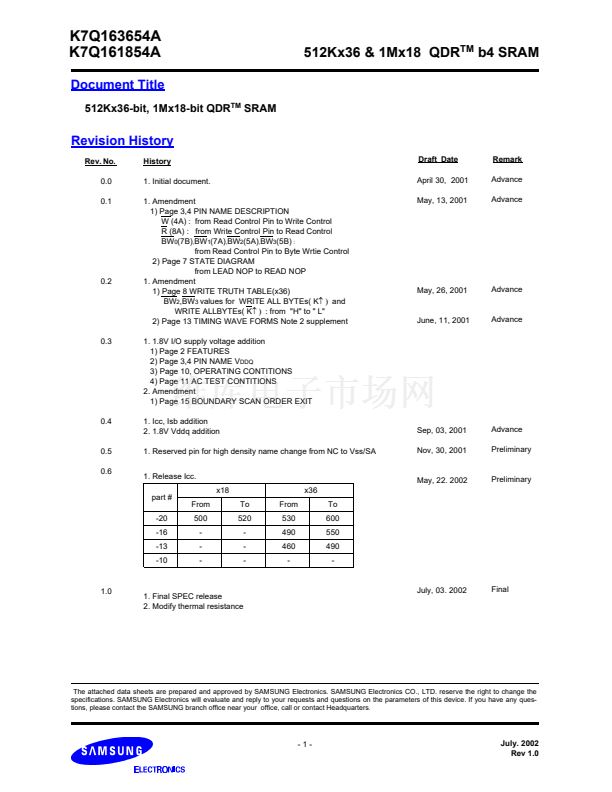
1. Release Icc.
part #
-20
-16
-13
-10
x18
From
500
-
-
-
To
520
-
-
-
From
530
490
460
-
x36
To
600
550
490
-
Draft Date
April 30, 2001
May, 13, 2001
Remark
Advance
Advance
0.2
May, 26, 2001
Advance
June, 11, 2001
Advance
0.3
0.4
Sep, 03, 2001
Nov, 30, 2001
Advance
Preliminary
0.5
0.6
May, 22. 2002
Preliminary
1.0
1. Final SPEC release
2. Modify thermal resistance
July, 03. 2002
Final
The attached data sheets are prepared and approved by SAMSUNG Electronics. SAMSUNG Electronics CO., LTD. reserve the right to change the
specifications. SAMSUNG Electronics will evaluate and reply to your requests and questions on the parameters of this device. If you have any ques-
tions, please contact the SAMSUNG branch office near your office, call or contact Headquarters.
-1-
July. 2002
Rev 1.0


 1
1
 2
2
 3
3
 4
4
 5
5
 6
6
 7
7
 8
8
 9
9
 10
10
 11
11
 12
12
 13
13
 14
14
 15
15
 16
16
 17
17
