鈩?/div>
Clamped inductive load, L = 30
碌H
T
C
= 25擄C
Maximum Ratings
600
600
鹵20
鹵30
75
50
200
I
CM
= 100
@ 0.8 V
CES
300
-55 ... +150
150
-55 ... +150
6
300
V
V
V
V
A
A
A
A
W
擄C
擄C
擄C
g
擄C
l
G
E
C (TAB)
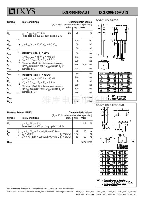
TO-247 Hole-less
(50N60AU1)
C (TAB)
G
C
C = Collector,
TAB = Collector
G = Gate,
E = Emitter,
Features
l
l
l
l
Maximum lead temperature for soldering
1.6 mm (0.062 in.) from case for 10 s
l
Hole-less TO-247 for clip mount
High current capability
High frequency IGBT and anti-
parallel FRED in one package
Low V
CE(sat)
- for minimum on-state conduction
losses
MOS Gate turn-on
- drive simplicity
Fast Recovery Epitaxial Diode (FRED)
- soft recovery with low I
RM
Applications
Symbol
Test Conditions
Characteristic Values
(T
J
= 25擄C, unless otherwise specified)
min. typ. max.
600
2.5
T
J
= 25擄C
T
J
= 125擄C
5.5
250
15
鹵100
2.7
V
V
碌A
mA
nA
V
l
l
l
BV
CES
V
GE(th)
I
CES
I
GES
V
CE(sat)
I
C
I
C
= 500
碌A,
V
GE
= 0 V
= 500
碌A,
V
CE
= V
GE
l
l
AC motor speed control
DC servo and robot drives
DC choppers
Uninterruptible power supplies (UPS)
Switch-mode and resonant-mode
power supplies
V
CE
= 0.8 鈥?V
CES
V
GE
= 0 V
V
CE
= 0 V, V
GE
=
鹵20
V
I
C
= I
C90
, V
GE
= 15 V
Advantages
l
l
l
Space savings (two devices in one
package)
Reduces assembly time and cost
High power density
漏 1997 IXYS All rights reserved
97513 (5/97)


 1
1
 2
2
 3
3
 4
4
 5
5
 6
6
