鈥?Reprogram Soldered Devices for Faster Prototyping
Copyright 漏 2002 Lattice Semiconductor Corp. All brand or product names are trademarks or registered trademarks of their respective holders. The specifications and information herein are subject
to change without notice.
U
SE
is
p
FO
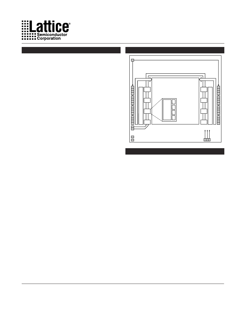
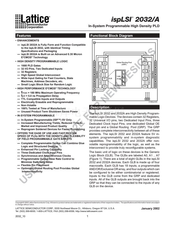
The ispLSI 2032 and 2032A are High Density Program-
mable Logic Devices. The devices contain 32 Registers,
32 Universal I/O pins, two Dedicated Input Pins, three
Dedicated Clock Input Pins, one dedicated Global OE
input pin and a Global Routing Pool (GRP). The GRP
provides complete interconnectivity between all of these
elements. The ispLSI 2032 and 2032A feature 5V in-
system programmability and in-system diagnostic
capabilities. The ispLSI 2032 and 2032A offer non-
volatile reprogrammability of the logic, as well as the
interconnect to provide truly reconfigurable systems.
The basic unit of logic on these devices is the Generic
Logic Block (GLB). The GLBs are labeled A0, A1 .. A7
(Figure 1). There are a total of eight GLBs in the ispLSI
2032 and 2032A devices. Each GLB is made up of four
macrocells. Each GLB has 18 inputs, a programmable
AND/OR/Exclusive OR array, and four outputs which can
be configured to be either combinatorial or registered.
Inputs to the GLB come from the GRP and dedicated
inputs. All of the GLB outputs are brought back into the
GRP so that they can be connected to the inputs of any


 1
1
 2
2
 3
3
 4
4
 5
5
 6
6
 7
7
 8
8
 9
9
 10
10
 11
11
 12
12
 13
13
 14
14
 15
15
