0.040鈩?/div>
I
D
56A
Benefits
l
Low Gate-to-Drain Charge to Reduce Switching Losses
l
Fully Characterized Capacitance Including Effective C
OSS
to
Simplify Design, (See App. Note AN1001)
l
Fully Characterized Avalanche Voltage and Current
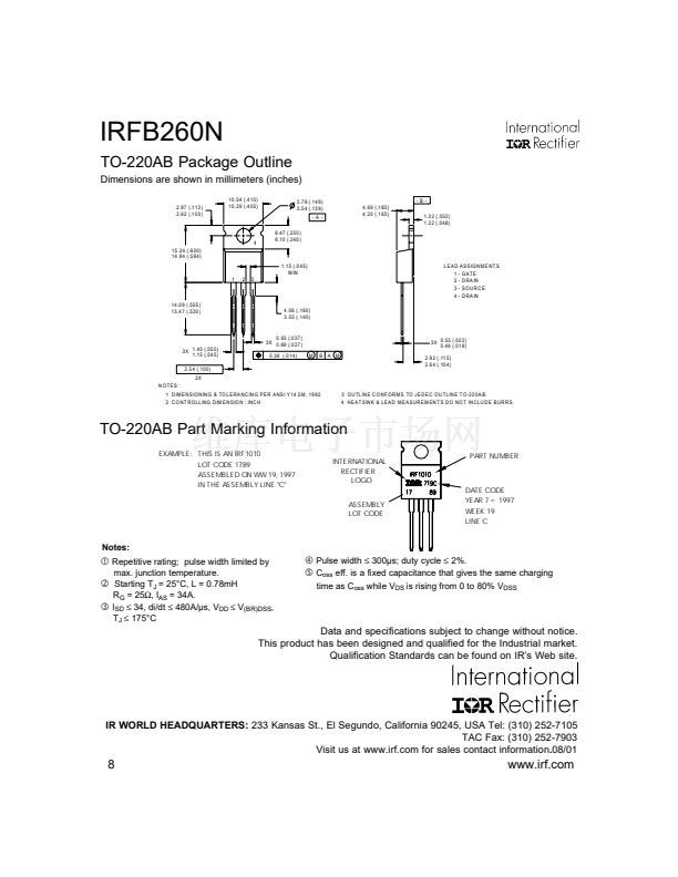
TO-220AB
Absolute Maximum Ratings
Parameter
I
D
@ T
C
= 25擄C
I
D
@ T
C
= 100擄C
I
DM
P
D
@T
C
= 25擄C
V
GS
dv/dt
T
J
T
STG
Continuous Drain Current, V
GS
@ 10V
Continuous Drain Current, V
GS
@ 10V
Pulsed Drain Current
聛
Power Dissipation
Linear Derating Factor
Gate-to-Source Voltage
Peak Diode Recovery dv/dt
聝
Operating Junction and
Storage Temperature Range
Soldering Temperature, for 10 seconds
Mounting torqe, 6-32 or M3 screw
Max.
56
40
220
380
2.5
鹵 20
10
-55 to + 175
300 (1.6mm from case )
10 lbf鈥n (1.1N鈥)
Units
A
W
W/擄C
V
V/ns
擄C
Thermal Resistance
Parameter
R
胃JC
R
胃CS
R
胃JA
Junction-to-Case
Case-to-Sink, Flat, Greased Surface
Junction-to-Ambient
Typ.
鈥撯€撯€?/div>
0.50
鈥撯€撯€?/div>
Max.
0.40
鈥撯€撯€?/div>
62
Units
擄C/W
Notes
聛
through
聟
are on page 8
www.irf.com
1
8/29/01


 1
1
 2
2
 3
3
 4
4
 5
5
 6
6
 7
7
 8
8
