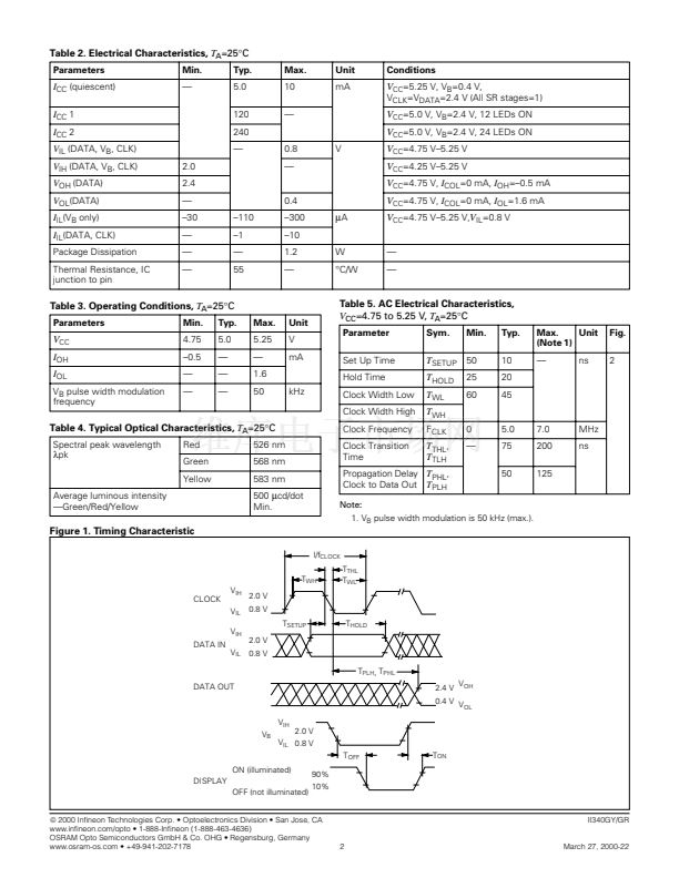
GREEN and YELLOW, GREEN and RED
3 x 4 Cells, Bi-Color Intelligent Indicators
Dimensions in inches (mm)
.020 (.50)
1
.288
(5.80)
.680 typ.
(17.30)
.909 (23.10)
2
3
4
.020 (.50)
II340GY/GR
5
6
7
8
.226
(5.74)
9
.288
(5.80)
typ.
10
11
12
.157 (4.00) sq.
typ.
PIN 1
.220 (5.59)
S YYWW
pin 1
.205
(5.21)
II340GY
.160
鹵.020
(4.06
鹵.50)
FEATURES
鈥?Colors: GY=Green and Yellow,
GR=Green and Red
鈥?Each Cell, 4.0 mm square
鈥?Vertical and Horizontal Pitch, 5.8 mm
鈥?X-Y Stackable
鈥?TTL Compatible
鈥?Easily Cascaded for Multiple Displays
鈥?Ideal for Graphics Panels
DESCRIPTION
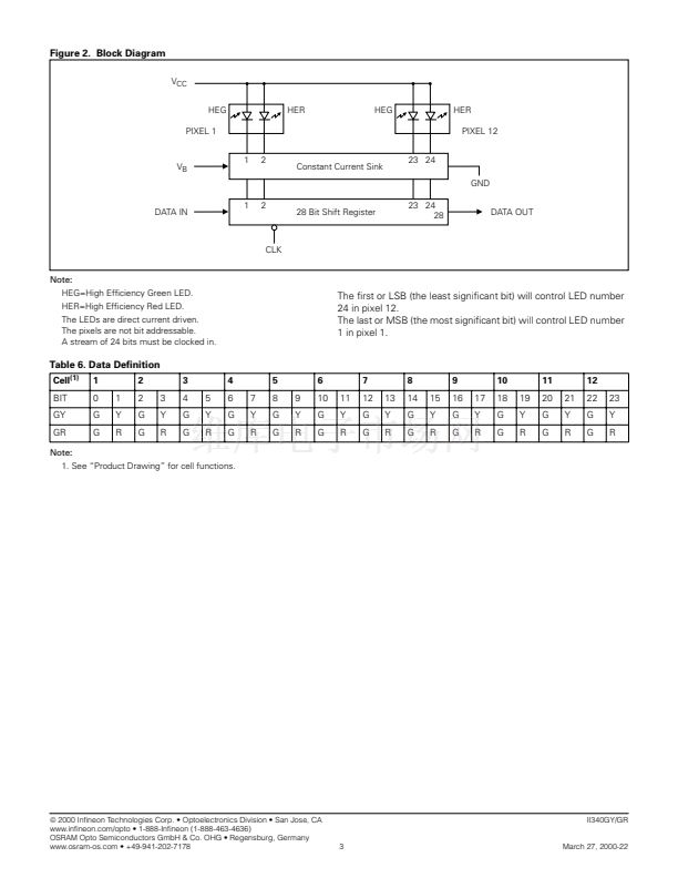
The II340GY/GR bi-color intelligent indicator is a 3 x 4
cell assembly with a built-in CMOS shift register and
LED drivers. Each cell or pixel has a green and yellow
LED (GY) or a green and red LED (GR). To turn a LED
鈥淥N鈥?a 1 (high) has to be clocked into the respective
shift register (see the block diagram). The serial clock
has to be provided to pin 4, the 鈥渟hift register clock.鈥?/div>
The serial data bit stream is clocked in on the falling
edge of the clock pulses.
The blanking pin can be used to blank the indicator
while the data is being updated and it can also be
pulse width modulated to dim the display and con-
sume less power.
Cascading multiple indicators is possible because of
the data out and data in pins. Notice in the block dia-
gram that only 24 LED drivers are used while 28 shift
registers are available. So when multiple indicators are
cascaded data for the next indicator will only be at the
data out pin after the twenty eighth clock pulse.
.100
(2.54)
typ.
.018 (.46) sq.
typ.
TOL: 0.XX (0.XXX)=鹵0.25 (0.010)
Absolute Maximum Ratings,
T
A
=25擄C
DC Supply Voltage .......................................................... 鈥?.5 V to +7.0 V
Input Voltage Levels Relative to GND.......................鈥?.5 V to
V
CC
+0.5 V
Operating/Storage Temperature Range ........................... 鈥?0擄C to +85擄C
Maximum solder Temperature 0.063 in (1.59 mm) below
Seating Plane t<5.0 sec. ............................................................. 260擄C
Table 1. Pin Function/Description
Pin
1
2
3
4
5
6
Function
GND
Data Out
Blanking
Serial Clock
Data In
Description
Ground
Serial data output for cascading
Blanking control to enable or disable display
Shift register clock
Serial data input
+5.0 V supply
V
CC
Custom overlays are available from:
1-800-279-6001
Actual size
1
A
2
B
3
C
4
D
1 2 3
A B C
攏
"
+
i
錚?/div>
2000 In鏗乶eon Technologies Corp. 鈥?Optoelectronics Division 鈥?San Jose, CA
www.in鏗乶eon.com/opto 鈥?1-888-In鏗乶eon (1-888-463-4636)
OSRAM Opto Semiconductors GmbH & Co. OHG 鈥?Regensburg, Germany
www.osram-os.com 鈥?+49-941-202-7178
1
March 27, 2000-22


 1
1
 2
2
 3
3
