鈥?/div>
For group skew timing, please refer to the
Group Timing Relationship Table.
VDDA
GNDA
X1
X2
GND3V66
VDD3V66
3V66-0
3V66-1
3V66-2
VDDPCI
GNDPCI
1
*FS0/PCICLK0
1
*FS1/PCICLK1
1
*SEL24_48#/PCICLK2
GNDPCI
VDDPCI
PCICLK3
PCICLK4
PCICLK5
PCICLK6
RATIO_0
PD#
SCLK
SDATA
VDD48
GND48
*FS2/24_48MHz
1
*FS3/48MHz
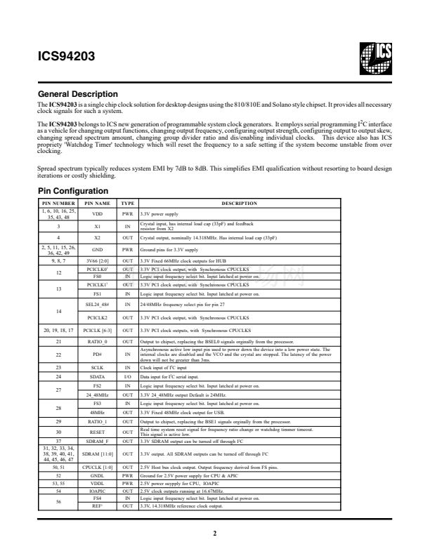
Pin Configuration
1
2
3
4
5
6
7
8
9
10
11
12
13
14
15
16
17
18
19
20
21
22
23
24
25
26
27
28
56
55
54
53
52
51
50
49
48
47
46
45
44
43
42
41
40
39
38
37
36
35
34
33
32
31
30
29
REF/FS4*
VDDLAPIC
1
IOAPIC0
VDDLCPU
GNDLCPU
CPUCLK0
CPUCLK1
GNDSDR
VDDSDR
SDRAM0
SDRAM1
SDRAM2
SDRAM3
VDDSDR
GNDSDR
SDRAM4
SDRAM5
SDRAM6
SDRAM7
SDRAM_F
GNDSDR
VDDSDR
SDRAM8
SDRAM9
SDRAM10
SDRAM11
RESET#
RATIO_1
1
56-Pin 300 mil SSOP
1. These pins will have 1.5 to 2X drive strength.
* 120K ohm pull-up to VDD on indicated inputs.
Block Diagram
PLL2
/2
X1
X2
XTAL
OSC
PLL1
Spread
Spectrum
CPU
DIVDER
SDRAM
DIVDER
2
ICS94203
48MHz
24_48MHz
REF
CPUCLK (1:0)
SDRAM (11:0)
SDRAM_F
IOAPIC
DIVDER
12
Power Groups
VDDA, GNDA = Core PLL, Xtal
VDD48, GND48 = 48MHz, Fixed PLL
FS(4:0)
PD#
SEL24_48#
SDATA
SCLK
Control
Logic
Config.
Reg.
IOAPIC
PCICLK (6:0)
3V66 (2:0)
RESET#
RATIO_0
RATIO_1
PCI
DIVDER
3V66
DIVDER
7
3
94203 Rev B 02/13/01
ICS reserves the right to make changes in the device data identified in
this publication without further notice. ICS advises its customers to
obtain the latest version of all device data to verify that any
information being relied upon by the customer is current and accurate.


 1
1
 2
2
 3
3
 4
4
 5
5
 6
6
 7
7
 8
8
 9
9
 10
10
 11
11
 12
12
 13
13
 14
14
 15
15
 16
16
 17
17
 18
18
