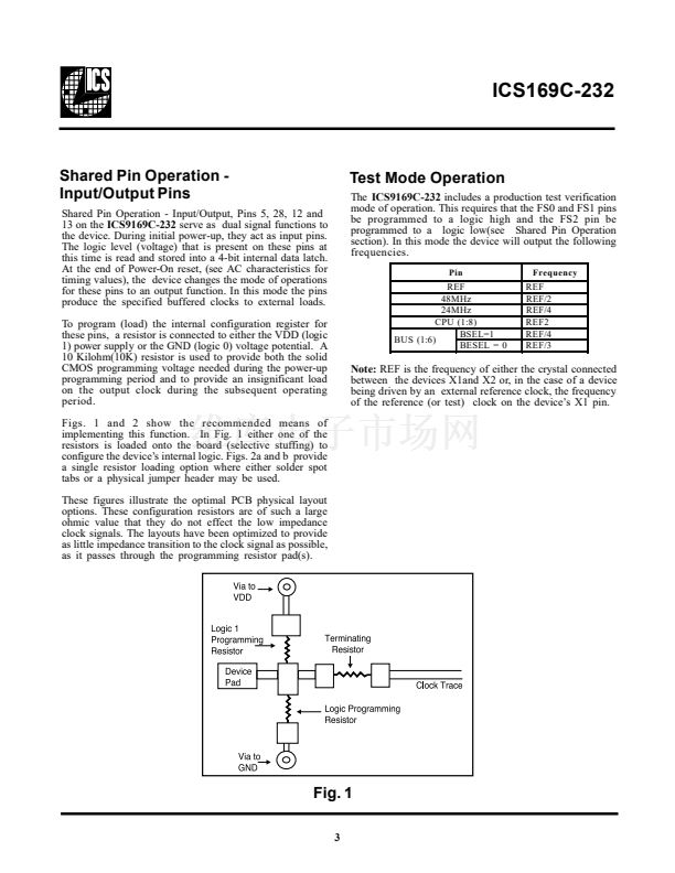
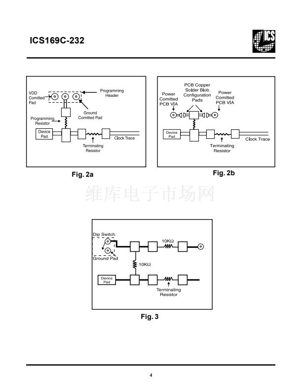
鈥?/div>
Strong output drive.
Eight selectable CPU clocks operate up to 83.3 MHz
Frequency selections include Turbo-mode speed of 68.5
MHz
Maximum CPU jitter of 鹵200ps
Six BUS clocks support sync or async bus operation
250ps skew window for CPU outputs, 500ps skew window for
BUS outputs
CPU clocks to BUS clocks skew 1-4 ns (CPU early)
48 MHz clock for USB support & 24 MHz clock for FD.
Logic inputs latched at Power-On for frequency selection
saving pins as Input/Output
Integrated buffer outputs drive up to 30pF loads
3.0V - 3.7V supply range, CPU (1:6) outputs 2.5V
(2.375 - 2.6V) VDD option
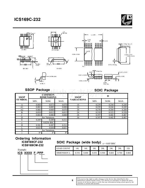
28-pin SOIC or SSOP package
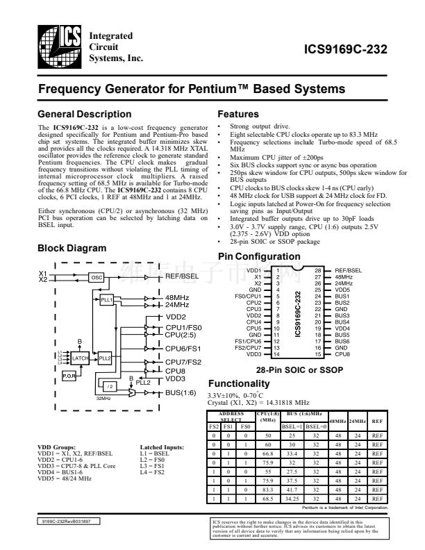
Block Diagram
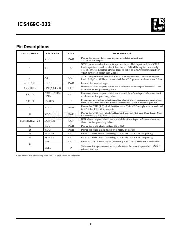
Pin Configuration
28-Pin SOIC or SSOP
Functionality
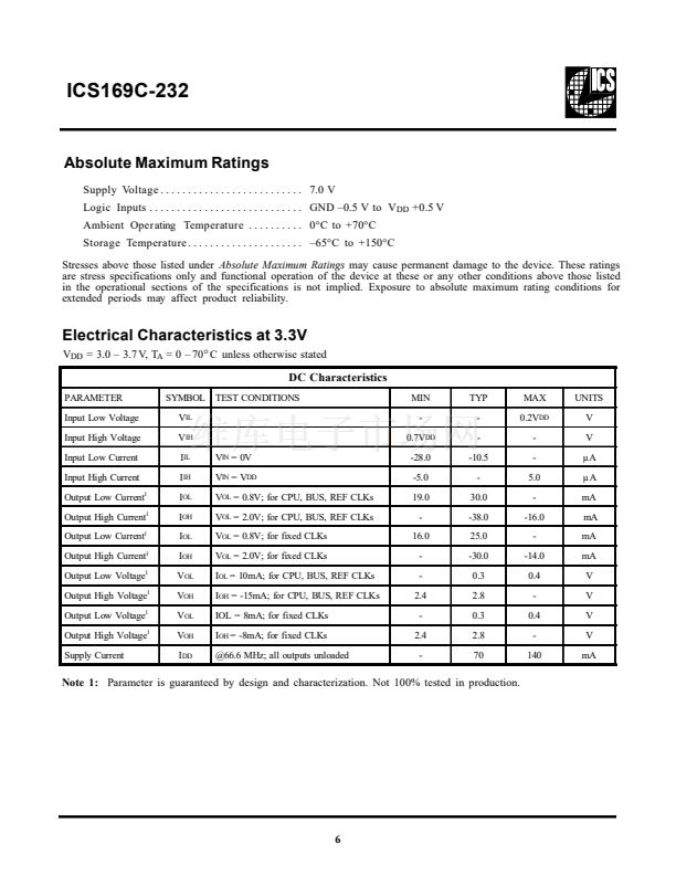
3.3V鹵10%, 0-70
擄
C
Crystal (X1, X2) = 14.31818 MHz
ADD RESS
SEL ECT
CP U(1:8)
(MHz)
BU S (1:6)MHz
48MHz 24MHz
RE F
FS2 FS1
0
0
0
1
1
0
0
1
1
0
0
0
1
1
1
1
FS0
0
1
0
1
0
1
0
1
50
60
66.8
75.9
55
75.9
83.3
68.5
BSEL=1 BSEL=0
25
30
33.4
32
27.5
37.5
41.7
34.25
32
32
32
32
32
32
32
32
48
48
48
48
48
48
48
48
24
24
24
24
24
24
24
24
REF
REF
REF
REF
REF
REF
REF
REF
VDD Groups:
VDD1 = X1, X2, REF/BSEL
VDD2 = CPU1-6
VDD3 = CPU7-8 & PLL Core
VDD4 = BUS1-6
VDD5 = 48/24 MHz
Latched Inputs:
L1 = BSEL
L2 = FS0
L3 = FS1
L4 = FS2
Pentium is a trademark of Intel Corporation.
9169C-232RevB031897
ICS reserves the right to make changes in the device data identified in this
publication without further notice. ICS advises its customers to obtain the latest
version of all device data to verify that any information being relied upon by the
customer is current and accurate.


 1
1
 2
2
 3
3
 4
4
 5
5
 6
6
 7
7
 8
8
