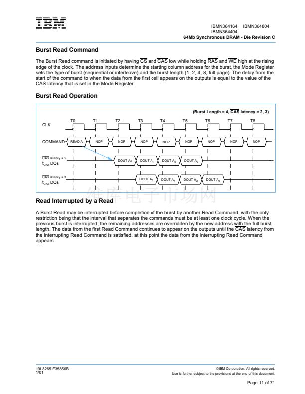
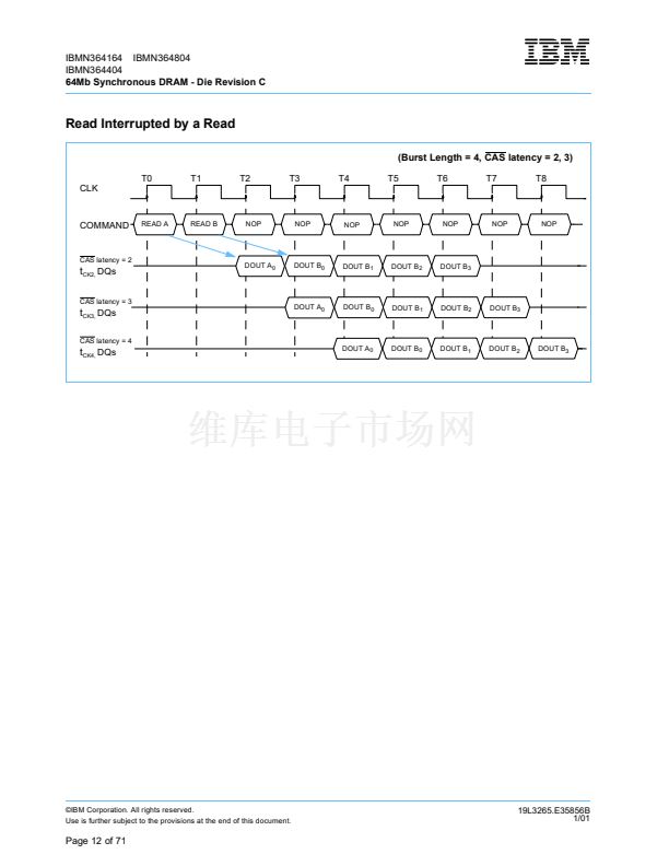
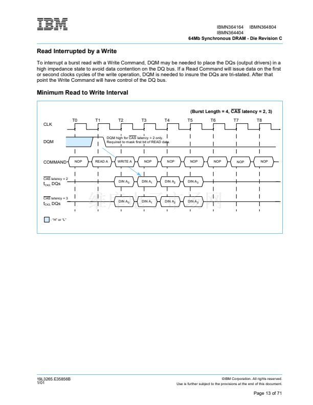
鈥?/div>
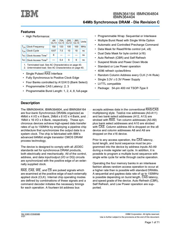
1. Terminated load. See AC Characteristics on page 40.
2. Unterminated load. See AC Characteristics on page 40.
鈥?Single Pulsed RAS Interface
鈥?Fully Synchronous to Positive Clock Edge
鈥?Four Banks controlled by A12/A13 (Bank Select)
鈥?Programmable CAS Latency: 2, 3
鈥?Programmable Burst Length: 1, 2, 4, 8, full-page
Description
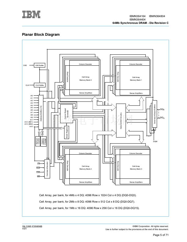
The IBMN364404, IBMN364804, and IBMN364164
are four-bank Synchronous DRAMs organized as
4Mbit x 4 I/O x 4 Bank, 2Mbit x 8 I/O x 4 Bank, and
1Mbit x 16 I/O x 4 Bank, respectively. These syn-
chronous devices achieve high-speed data transfer
rates of up to 150MHz by employing a pipeline chip
architecture that synchronizes the output data to a
system clock. The chip is fabricated with IBM鈥檚
advanced 64Mbit single transistor CMOS DRAM
process technology.
The device is designed to comply with all JEDEC
standards set for synchronous DRAM products,
both electrically and mechanically. All of the control,
address, and data input/output (I/O or DQ) circuits
are synchronized with the positive edge of an exter-
nally supplied clock.
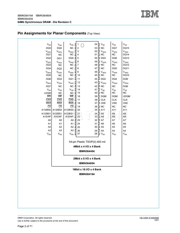
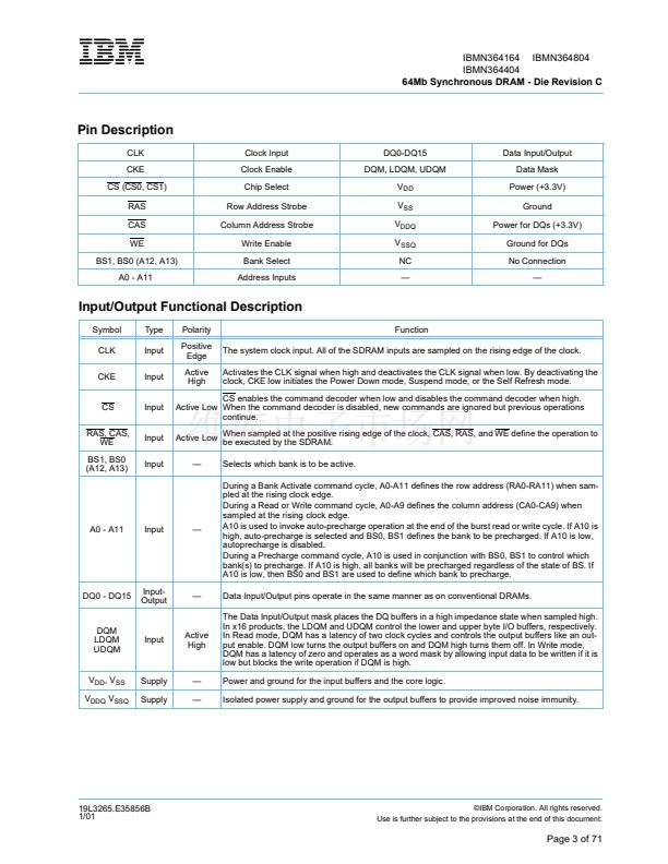
RAS, CAS, WE, and CS are pulsed signals which
are examined at the positive edge of each externally
applied clock (CLK). Internal chip operating modes
are defined by combinations of these signals and a
command decoder initiates the necessary timings
for each operation. A fourteen bit address bus
accepts address data in the conventional RAS/CAS
multiplexing style. Twelve row addresses (A0-A11)
and two bank select addresses (A12, A13) are
strobed with RAS. Ten column addresses (A0-A9)
plus bank select addresses and A10 are strobed
with CAS. Column address A9 is dropped on the x8
device and column addresses A8 and A9 are
dropped on the x16 device.
Prior to any access operation, the CAS latency,
burst length, and burst sequence must be pro-
grammed into the device by address inputs A0-A9
during a mode register set cycle. In addition, it is
possible to program a multiple burst sequence with
single write cycle for write through cache operation.
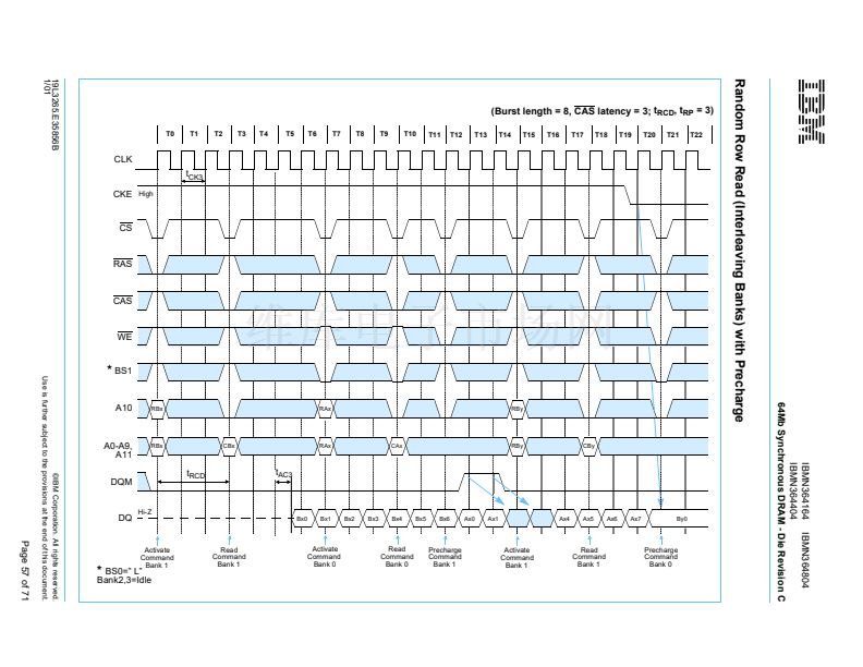
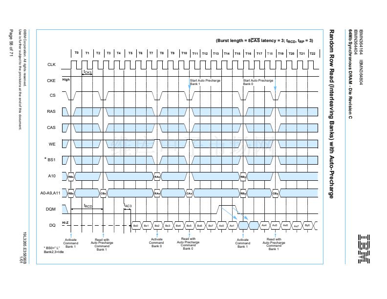
Operating the four memory banks in an interleave
fashion allows random access operation to occur at
a higher rate than is possible with standard DRAMs.
A sequential and gapless data rate of up to 150MHz
is possible depending on burst length, CAS latency,
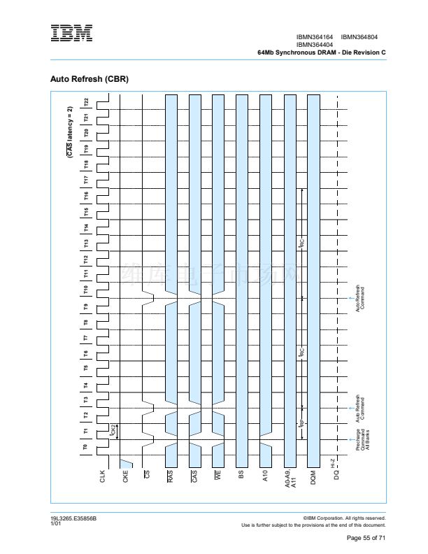
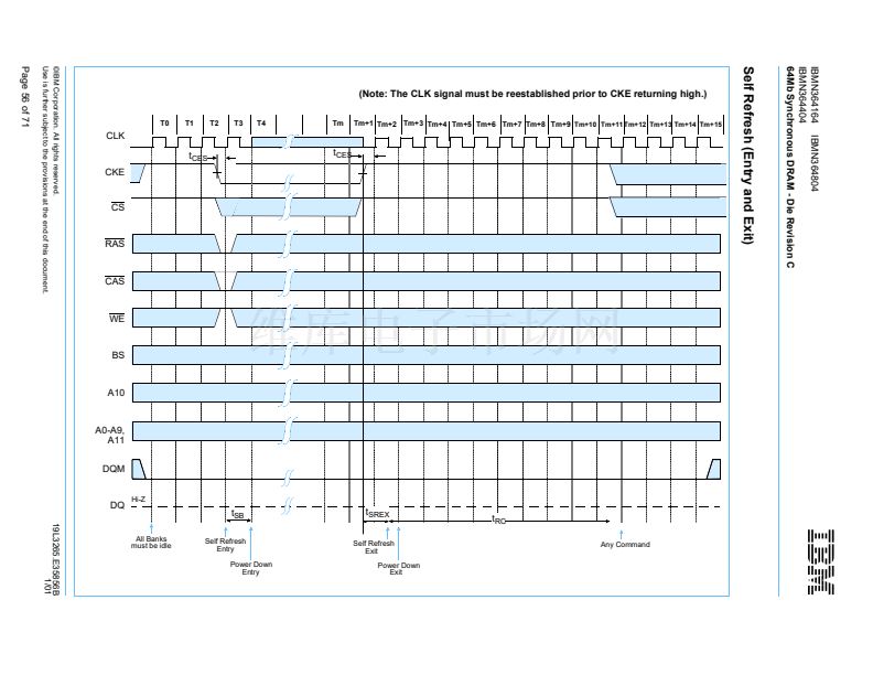
and speed grade of the device. Auto Refresh (CBR),
Self Refresh, and Low Power operation are sup-
ported.
19L3265.E35856B
1/01
漏IBM Corporation. All rights reserved.
Use is further subject to the provisions at the end of this document.
Page 1 of 71


 1
1
 2
2
 3
3
 4
4
 5
5
 6
6
 7
7
 8
8
 9
9
 10
10
 11
11
 12
12
 13
13
 14
14
 15
15
 16
16
 17
17
 18
18
 19
19
 20
20
 21
21
 22
22
 23
23
 24
24
 25
25
 26
26
 27
27
 28
28
 29
29
 30
30
 31
31
 32
32
 33
33
 34
34
 35
35
 36
36
 37
37
 38
38
 39
39
 40
40
 41
41
 42
42
 43
43
 44
44
 45
45
 46
46
 47
47
 48
48
 49
49
 50
50
 51
51
 52
52
 53
53
 54
54
 55
55
 56
56
 57
57
 58
58
 59
59
 60
60
 61
61
 62
62
 63
63
 64
64
 65
65
 66
66
 67
67
 68
68
 69
69
 70
70
 71
71
