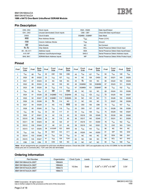
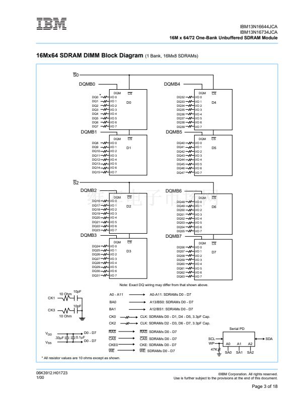
.
IBM13N16644JCA
IBM13N16734JCA
16M x 64/72 One-Bank Unbuffered SDRAM Module
Features
鈥?168-Pin Unbuffered 8-Byte Dual In-Line Memory
Module
鈥?Intended for PC100 applications
鈥?Clock Frequency: 100MHz
鈥?Clock Cycle: 10.0ns
鈥?-260 and -360 speed sorts
鈥?Inputs and outputs are LVTTL (3.3V) compatible
鈥?Single 3.3V
鹵
0.3V Power Supply
鈥?Single Pulsed RAS interface
鈥?SDRAMs have four internal banks
鈥?Module has one physical bank
鈥?Fully Synchronous to positive Clock Edge
鈥?Data Mask for Byte Read/Write control
鈥?Auto Refresh (CBR) and Self Refresh
鈥?Automatic and controlled Precharge commands
鈥?Programmable Operation:
- CAS Latency: 2, 3
- Burst Type: Sequential or Interleave
- Burst Length: 1, 2, 4, 8, Full-Page
(Full-Page supports Sequential burst only)
- Operation: Burst Read and Write or Multiple
Burst Read with Single Write
鈥?Suspend Mode and Power Down Mode
鈥?12/10/2 Addressing (Row/Column/Bank)
鈥?4096 Refresh cycles distributed across 64ms
鈥?Card size: 5.25" x 1.375" x 0.106"
鈥?Gold contacts
鈥?SDRAMs in TSOP Type II Package
鈥?Serial Presence Detect with Write Protect
Description
IBM13N16644JCA / IBM13N16734JCA are unbuf-
fered 168-pin Synchronous DRAM Dual In-Line
Memory Modules (DIMMs) which are organized as
16Mx64 and 16Mx72 high-speed memory arrays
and are configured as one 16M x 64/72 physical
bank. The DIMMs use eight (16Mx64) or nine
(16Mx72) 16Mx8 SDRAMs in 400mil TSOP II pack-
ages. The DIMMs achieve high-speed data transfer
rates of up to 100MHz by employing a prefetch/pipe-
line hybrid architecture that supports the JEDEC 1N
rule while allowing very low burst power.
All control, address, and data input/output circuits
are synchronized with the positive edge of the exter-
nally supplied clock inputs.
All inputs are sampled at the positive edge of each
externally supplied clock (CK0, CK2). Internal oper-
ating modes are defined by combinations of RAS,
CAS, WE, S0/S2, DQMB, and CKE0 signals. A
command decoder initiates the necessary timings
for each operation. A 14-bit address bus accepts
address information in a row/column multiplexing
arrangement.
Prior to any Access operation, the CAS latency,
burst type, burst length, and Burst operation type
must be programmed into the DIMM by address
inputs A0-A9 during the Mode Register Set cycle.
The DIMM uses serial presence detects imple-
mented via a serial EEPROM using the two-pin IIC
protocol. The first 128 bytes of serial PD data are
used by the DIMM manufacturer. The last 128 bytes
are available to the customer.
All IBM 168-pin DIMMs provide a high-performance,
flexible 8-byte interface in a 5.25" long space-saving
footprint. Related products include both EDO DRAM
and SDRAM unbuffered DIMMs in both non-parity
x64 and ECC-Optimized x72 configurations.
Card Outline
(Front)
(Back)
1
85
10 11
94 95
40 41
124 125
84
168
06K3912.H01723
1/00
漏IBM Corporation. All rights reserved.
Use is further subject to the provisions at the end of this document.
Page 1 of 18


 1
1
 2
2
 3
3
 4
4
 5
5
 6
6
 7
7
 8
8
 9
9
 10
10
 11
11
 12
12
 13
13
 14
14
 15
15
 16
16
 17
17
 18
18
