鈥?/div>
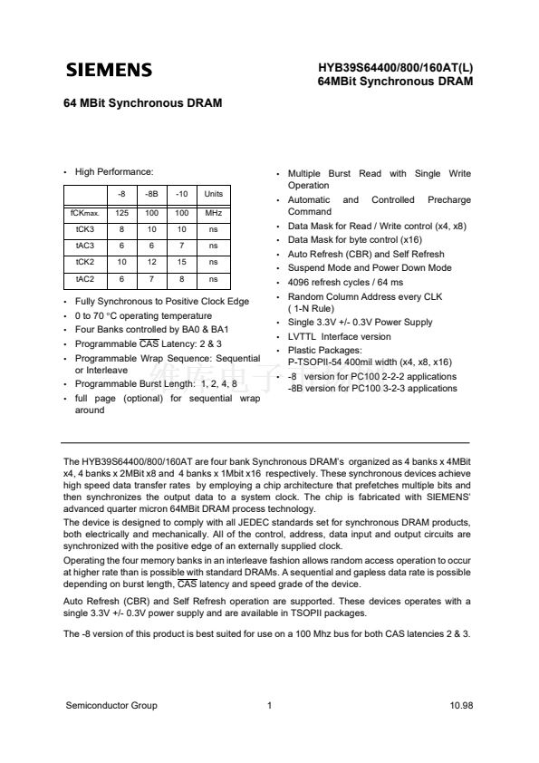
Fully Synchronous to Positive Clock Edge
0 to 70
擄C
operating temperature
Four Banks controlled by BA0 & BA1
Programmable CAS Latency: 2 & 3
Programmable Wrap Sequence: Sequential
or Interleave
Programmable Burst Length: 1, 2, 4, 8
full page (optional) for sequential wrap
around
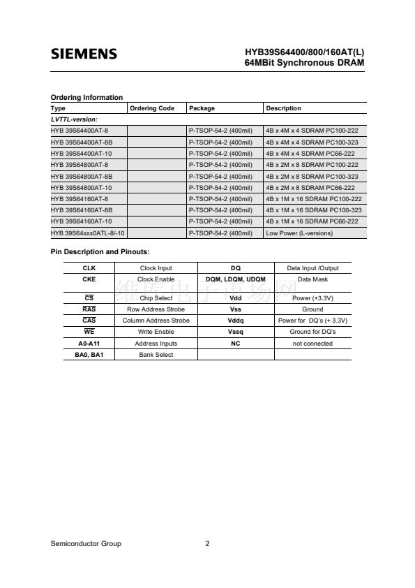
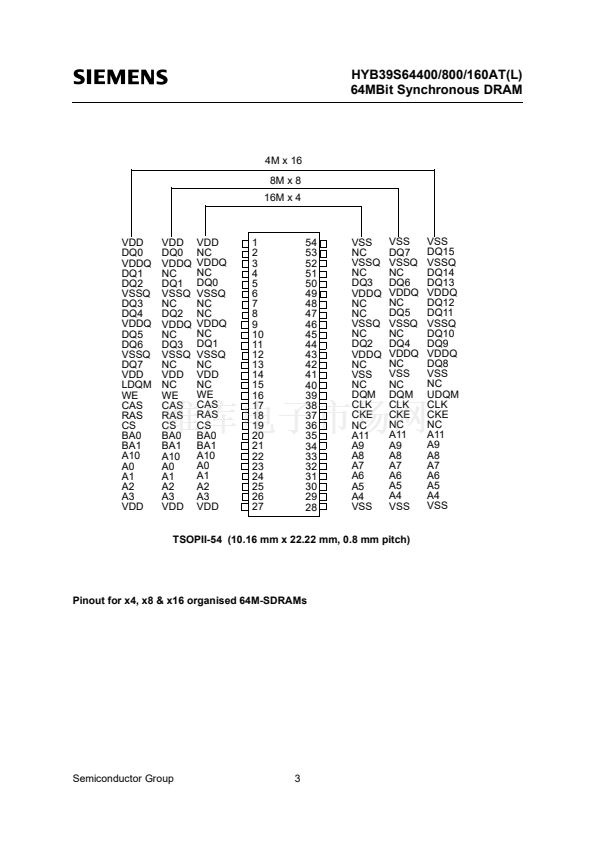
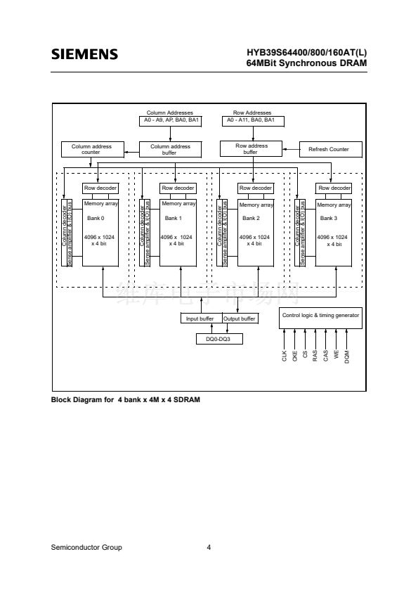
The HYB39S64400/800/160AT are four bank Synchronous DRAM鈥檚 organized as 4 banks x 4MBit
x4, 4 banks x 2MBit x8 and 4 banks x 1Mbit x16 respectively. These synchronous devices achieve
high speed data transfer rates by employing a chip architecture that prefetches multiple bits and
then synchronizes the output data to a system clock. The chip is fabricated with SIEMENS鈥?/div>
advanced quarter micron 64MBit DRAM process technology.
The device is designed to comply with all JEDEC standards set for synchronous DRAM products,
both electrically and mechanically. All of the control, address, data input and output circuits are
synchronized with the positive edge of an externally supplied clock.
Operating the four memory banks in an interleave fashion allows random access operation to occur
at higher rate than is possible with standard DRAMs. A sequential and gapless data rate is possible
depending on burst length, CAS latency and speed grade of the device.
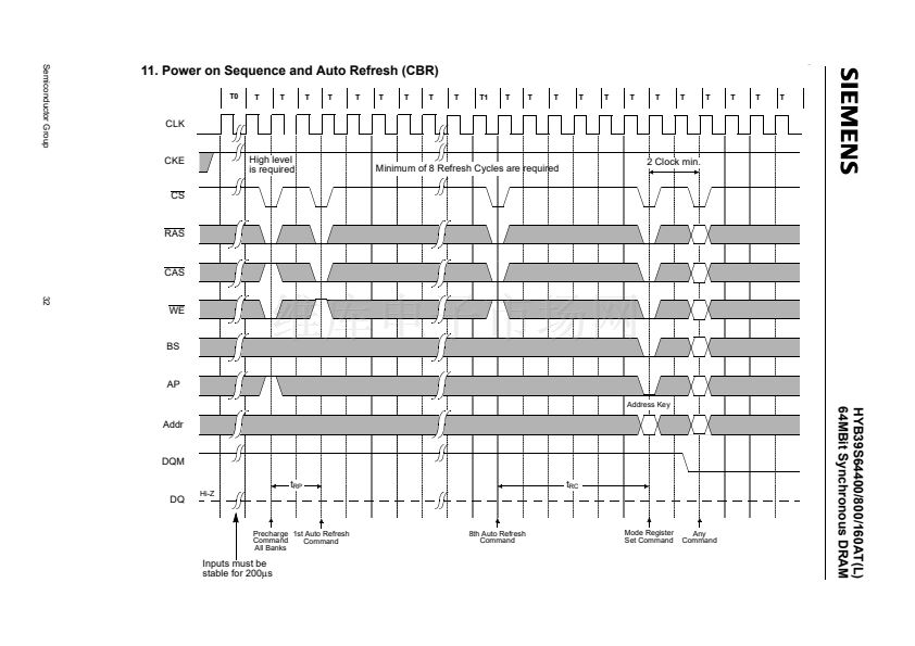
Auto Refresh (CBR) and Self Refresh operation are supported. These devices operates with a
single 3.3V +/- 0.3V power supply and are available in TSOPII packages.
The -8 version of this product is best suited for use on a 100 Mhz bus for both CAS latencies 2 & 3.
Semiconductor Group
1
10.98


 1
1
 2
2
 3
3
 4
4
 5
5
 6
6
 7
7
 8
8
 9
9
 10
10
 11
11
 12
12
 13
13
 14
14
 15
15
 16
16
 17
17
 18
18
 19
19
 20
20
 21
21
 22
22
 23
23
 24
24
 25
25
 26
26
 27
27
 28
28
 29
29
 30
30
 31
31
 32
32
 33
33
 34
34
 35
35
 36
36
 37
37
 38
38
 39
39
 40
40
 41
41
 42
42
 43
43
 44
44
 45
45
 46
46
 47
47
 48
48
 49
49
 50
50
 51
51
 52
52
 53
53
