HY57V641620HG-I Series
4 Banks x 1M x 16Bit Synchronous DRAM
DESCRIPTION
The Hynix HY57V641620HG is a 67,108,864-bit CMOS Synchronous DRAM, ideally suited for the Mobile applications r which require
low power consumption and extended temperature range. HY57V641620HG is organized as 4banks of 1,048,576x16.
HY57V641620HG is offering fully synchronous operation referenced to a positive edge of the clock. All inputs and outputs are synchro-
nized with the rising edge of the clock input. The data paths are internally pipelined to achieve very high bandwidth. All input and output
voltage levels are compatible with LVTTL.
Programmable options include the length of pipeline (Read latency of 2 or 3), the number of consecutive read or write cycles initiated
by a single control command (Burst length of 1,2,4,8 or Full page), and the burst count sequence(sequential or interleave). A burst of
read or write cycles in progress can be terminated by a burst terminate command or can be interrupted and replaced by a new burst
read or write command on any cycle. (This pipelined design is not restricted by a `2N` rule.)
FEATURES
鈥?/div>
鈥?/div>
鈥?/div>
Single 3.3鹵0.3V power supply
Note)
All device pins are compatible with LVTTL interface
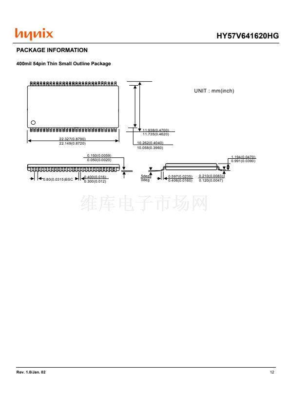
JEDEC standard 400mil 54pin TSOP-II with 0.8mm
of pin pitch
All inputs and outputs referenced to positive edge of
system clock
Data mask function by UDQM or LDQM
Internal four banks operation
鈥?/div>
鈥?/div>
鈥?/div>
鈥?/div>
Auto refresh and self refresh
4096 refresh cycles / 64ms
Programmable Burst Length and Burst Type
- 1, 2, 4, 8 or Full page for Sequential Burst
- 1, 2, 4 or 8 for Interleave Burst
Programmable CAS Latency ; 2, 3 Clocks
鈥?/div>
鈥?/div>
鈥?/div>
ORDERING INFORMATION
Part No.
HY57V641620HGT-5I/55I/6I/7I
HY57V641620HGT-KI
HY57V641620HGT-HI
HY57V641620HGT-8I
HY57V641620HGT-PI
HY57V641620HGT-SI
HY57V641620HGLT-5I/55I/6I/7I
HY57V641620HGLT-KI
HY57V641620HGLT-HI
HY57V641620HGLT-8I
HY57V641620HGLT-PI
HY57V641620HGLT-SI
Clock Frequency
200/183/166/143MHz
133MHz
133MHz
125MHz
100MHz
100MHz
200/183/166/143MHz
133MHz
133MHz
125MHz
100MHz
100MHz
Power
Organization
Interface
Package
Normal
4Banks x 1Mbits
x16
LVTTL
400mil 54pin TSOP II
Low power
Note : VDD(Min) of HY57V641620HG(L)T-5I/55I/6I is 3.135V
This document is a general product description and is subject to change without notice. Hynix Semiconductor does not assume any responsibility for use
of circuits described. No patent licenses are implied.
Rev. 1.0/Jan. 02
1
HY57V641620HG-I相關(guān)型號(hào)PDF文件下載
-
型號(hào)
版本
描述
廠商
下載
-
英文版
4 Banks x 8M x 8Bit Synchronous DRAM
HYNIX [Hyn...
-
英文版
Analog IC
ETC
-
英文版
Analog IC
ETC
-
英文版
Analog IC
ETC
-
英文版
Analog IC
ETC
-
英文版
Analog IC
ETC
-
英文版
Analog IC
ETC
-
英文版
4 Banks x 8M x 16Bit Synchronous DRAM
HYNIX [Hyn...
-
英文版
4 Banks x 1M x 32Bit Synchronous DRAM
HYNIX
-
英文版
4 Banks x 1M x 32Bit Synchronous DRAM
HYNIX [Hyn...
-
英文版
4Banks x 4M x 16Bit Synchronous DRAM
HYNIX
-
英文版
4Banks x 4M x 16Bit Synchronous DRAM
HYNIX [Hyn...
-
英文版
64Mx4|3.3V|8K|75|SDR SDRAM - 256M
ETC
-
英文版
4 Banks x 8M x 8Bit Synchronous DRAM
HYNIX [Hyn...
-
英文版
32Mx8|3.3V|8K|75|SDR SDRAM - 256M
ETC
-
英文版
8Mx8 bit Synchronous DRAM Series
HYNIX
-
英文版
8Mx8 bit Synchronous DRAM Series
HYNIX [Hyn...
-
英文版
8Mx8 bit Synchronous DRAM Series
HYNIX
-
英文版
8Mx8 bit Synchronous DRAM Series
HYNIX [Hyn...
-
英文版
8Mx8 bit Synchronous DRAM Series
HYNIX


 1
1
 2
2
 3
3
 4
4
 5
5
 6
6
 7
7
 8
8
 9
9
 10
10
 11
11
 12
12
