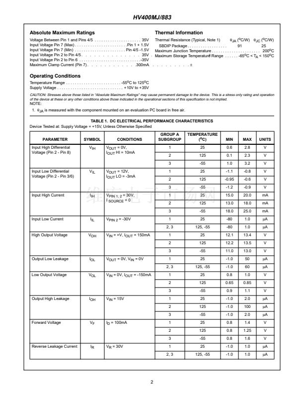
HV400MJ/883
August 1997
High Current MOSFET Driver
Description
The HV400MJ/883 is a single monolithic, non-inverting high
current driver designed to drive large capacitive loads at high
slew rates. The device is optimized for driving single or paral-
lel connected N-Channel power MOSFETs with total gate
charge from 5nC to >1000nC. It features two output stages
pinned out separately allowing independent control of the
MOSFET gate rise and fall times. The current sourcing output
stage is an NPN capable of 6A. An SCR provides over 30A of
current sinking. The HV400MJ/883 achieves rise and fall
times of 54ns and 16ns respectively driving a 10,000pF load.
Special features are included in this part to provide a simple,
high speed gate drive circuit for power MOSFETs. The
HV400MJ/883 requires no quiescent supply current, how-
ever, the input current is approximately 15mA while in the
high state. With the internal current steering diodes (Pin 7)
and an external capacitor, both the timing and MOSFET gate
power come from the same pulse transformer; no special
external supply is required for high side switches. No high
voltage diode is required to charge the bootstrap capacitor.
The HV400MJ/883 in combination with the MOSFET and
pulse transformer makes an isolated power switch building
block for applications such as high side switches, secondary
side regulation and synchronous recti鏗乧ation. The
HV400MJ/883 is also suitable for driving IGBTs, MCTs,
BJTs and small GTOs.
The HV400MJ/883 is a type of buffer; it does not have input
logic level switching threshold voltages. This single stage
design achieves propagation delays of 20ns. The output
NPN begins to source current when the voltage on Pin 2 is
approximately 2V more positive than the voltage at Pin 8.
The output SCR switches on when the input Pin 2 is 1V
more negative than the voltage at Pins 3/6. Due to the use of
the SCR for current sinking, once the output switches low,
the input must not go high again until all the internal SCR
charge has dissipated, 0.5碌s - 1.5碌s later.
Features
鈥?This Circuit is Processed in Accordance to MIL-STD-
883 and is Fully Conformant Under the Provisions of
Paragraph 1.2.1.
鈥?Fast Fall Times . . . . . . . . . . . . . . . . . . .16ns at 10,000pF
鈥?No Supply Current in Quiescent State
鈥?Peak Source Current . . . . . . . . . . . . . . . . . . . . . . . . . .6A
鈥?Peak Sink Current . . . . . . . . . . . . . . . . . . . . . . . . . . .30A
鈥?High Frequency Operation . . . . . . . . . . . . . . . . . 300kHz
Applications
鈥?Switch Mode Power Supplies
鈥?DC/DC Converters
鈥?Motor Controllers
鈥?Uninterruptable Power Supplies
Ordering Information
PART NUMBER
HV400MJ/883
TEMP.
RANGE (
o
C)
-55 to 125
PACKAGE
8 Ld SBDIP
PKG.
NO.
D8.3
Pinout
HV400MJ/883 (SBDIP)
TOP VIEW
Schematic
PIN 1
PIN 2
D3
D2
Q1
D1
PIN 8
PIN 7
PIN 3
D4
D8
R4
R2
PIN 6
V+ SUPPLY 1
INPUT 2
SINK OUTPUT 3
GND 4
8
7
6
5
SOURCE OUTPUT
DIODES
SINK OUTPUT
GND
Q2
R3
PIN 4
D6
R1
SCR
D7
PIN 5
CAUTION: These devices are sensitive to electrostatic discharge; follow proper IC Handling Procedures.
http://www.intersil.com or 407-727-9207
|
Copyright
漏
Intersil Corporation 1999
File Number
3584.2
1


 1
1
 2
2
 3
3
 4
4
 5
5
 6
6
 7
7
 8
8
 9
9
 10
10
 11
11
