HM-6508/883
March 1997
1024 x 1 CMOS RAM
Description
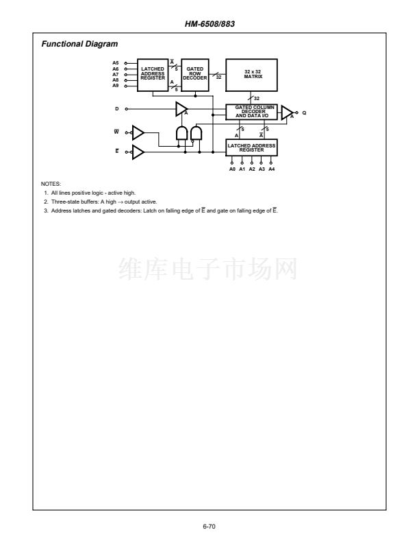
The HM-6508/883 is a 1024 x 1 static CMOS RAM
fabricated using self-aligned silicon gate technology.
Synchronous circuit design techniques are employed to
achieve high performance and low power operation.
On chip latches are provided for address allowing ef鏗乧ient
interfacing with microprocessor systems. The data output
buffers can be forced to a high impedance state for use in
expanded memory arrays.
The HM-6508/883 is a fully static RAM and may be main-
tained in any state for an inde鏗乶ite period of time. Data
retention supply voltage and supply current are guaranteed
over temperature.
Features
鈥?This Circuit is Processed in Accordance to
MIL-STD-883 and is Fully Conformant Under the Provi-
sions of Paragraph 1.2.1.
鈥?Low Power Standby . . . . . . . . . . . . . . . . . . . . 50碌W Max
鈥?Low Power Operation . . . . . . . . . . . . . 20mW/MHz Max
鈥?Fast Access Time. . . . . . . . . . . . . . . . . . . . . . 180ns Max
鈥?Data Retention . . . . . . . . . . . . . . . . . . . . . . . . . .2.0V Min
鈥?TTL Compatible Input/Output
鈥?High Output Drive - 2 TTL Loads
鈥?On-Chip Address Register
Ordering Information
PACKAGE
CERDIP
TEMP. RANGE
180ns
250ns
PKG. NO.
F16.3
-55
o
C to +125
o
C HM1-
HM1-
6508B/883 6508/883
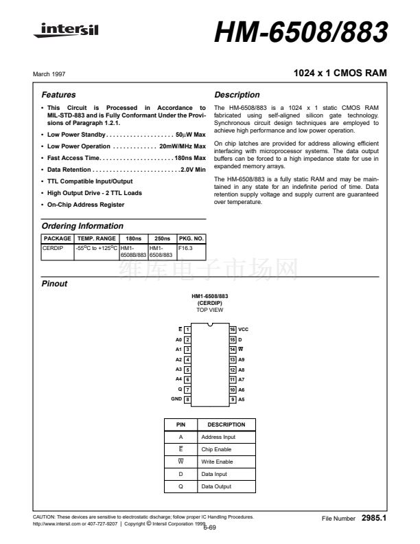
Pinout
HM1-6508/883
(CERDIP)
TOP VIEW
E 1
A0 2
A1 3
A2 4
A3 5
A4 6
Q 7
GND 8
16 VCC
15 D
14 W
13 A9
12 A8
11 A7
10 A6
9 A5
PIN
A
E
W
D
Q
DESCRIPTION
Address Input
Chip Enable
Write Enable
Data Input
Data Output
CAUTION: These devices are sensitive to electrostatic discharge; follow proper IC Handling Procedures.
http://www.intersil.com or 407-727-9207
|
Copyright
漏
Intersil Corporation 1999
File Number
2985.1
6-69


 1
1
 2
2
 3
3
 4
4
 5
5
 6
6
 7
7
 8
8
 9
9
