鈥?/div>
The GSM31P256KB-I66, and 256KB module, use GSI鈥檚
GS81132Q 32KX32 synchronous burst SRAM and a single
5V 8Kx8 SRAM for the tag. The GSM14P512K-I66, a
512KB module, use GSI鈥檚 GS82032Q 64KX32 synchronous
burst SRAM and a single 5V 32Kx8 SRAM for the tag.
The 3.3V data RAM and the 5V tag RAM provide an exact
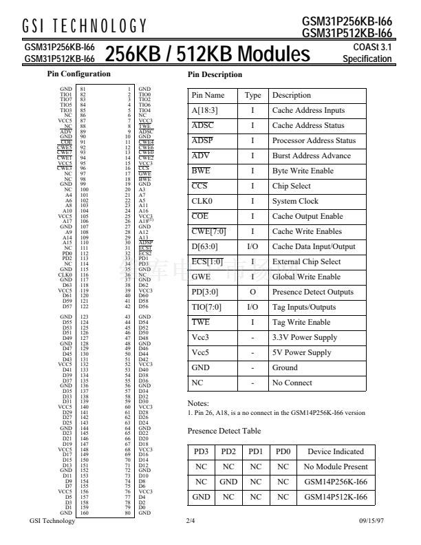
interface between the module and PC chip set. Four pres-
ence detect bits (PD) allow the system to recognize the type
of cache configuration present.
The low profile card edge package allows 160 signal leads
to be placed on a module, measuring 4.35 inches long, a
maximum of 0.310 inches thick and a maximum of 1.14
inches tall. This compact design allows the OEM to make
better use of the real estate on the mother-board for added
functions or smaller design for cost reduction.
All inputs and outputs and TTL compatible and operate
from two separate 5V and 3.3V power supplies. The use of
multiple ground pins and decoupling capacitors on-board
reduces failure due to noise.
Functional Description
The GSM31P256KB-I66 and the GSM31P512KB-I66 are
the secondary cache module designed for use with Intel Pen-
tium CPU based system. These modules use GSI鈥檚 Synchro-
nous Burst SRAMs in plastic surface mount packages
mounted on a multilayer epoxy laminate (FR-4) board.
Functional Block Diagram - GSM31P256KB-I66
TIO[7:0]
TWE
A[17:5]
D[7:0] 8kx8
WE
5V
A[12:0]
OE
CE CE
Vcc5
A[14:0]
OE
WE[3:0]
D[31:0]
ADSP
ADSC
ADV
CS
GWE
BWE
A[14:0]
OE
WE[3:0]
D[31:0]
ADSP
ADSC
ADV
CS
GWE
BWE
Power Supplies
32Kx32
Pipelined
Burst
SRAM
Functional Block Diagram - GSM31P512KB-I66
TIO[7:0]
TWE
A[18:5]
D[7:0] 16kx8
WE
5V
A[13:0]
OE
CE CE
Vcc5
A[15:0]
OE
WE[3:0]
D[31:0]
ADSP
ADSC
ADV
CS
GWE
BWE
A[15:0]
OE
WE[3:0]
D[31:0]
ADSP
ADSC
ADV
CS
GWE
BWE
64Kx32
Pipelined
Burst
SRAM
ECS2
ECS1
A[17:3]
COE
CWE[3:0]
D[31:0]
ADSP
ADSC
ADV
CCS
GWE
BWE
CE2
CE2
Vcc3
32Kx32
Pipelined
Burst
SRAM
ECS2
ECS1
A[18:3]
COE
CWE[3:0]
D[31:0]
ADSP
ADSC
ADV
CCS
GWE
BWE
CE2
CE2
Vcc3
64Kx32
Pipelined
Burst
SRAM
CWE[7:4]
D[63:32]
CLK0
PD[3:0]
CLK
NC
GND
CWE[7:4]
D[63:32]
CLK0
CE2
CE2
Vcc3
PD[3:0]
Vcc3,Vcc5
CLK
NC
GND
Power Supplies
CE2
CE2
Vcc3
Vcc3,Vcc5
GSI Technology
1/4
09/15/97


 1
1
 2
2
 3
3
 4
4
