鈥?/div>
JEDEC standard 100 lead package:
Q: QFP
T: TQFP
Pentium is a trademark of Intel Corp
.
GS820V32Q/T
80-133MHz (P/L)
66MHz Flow-Thru
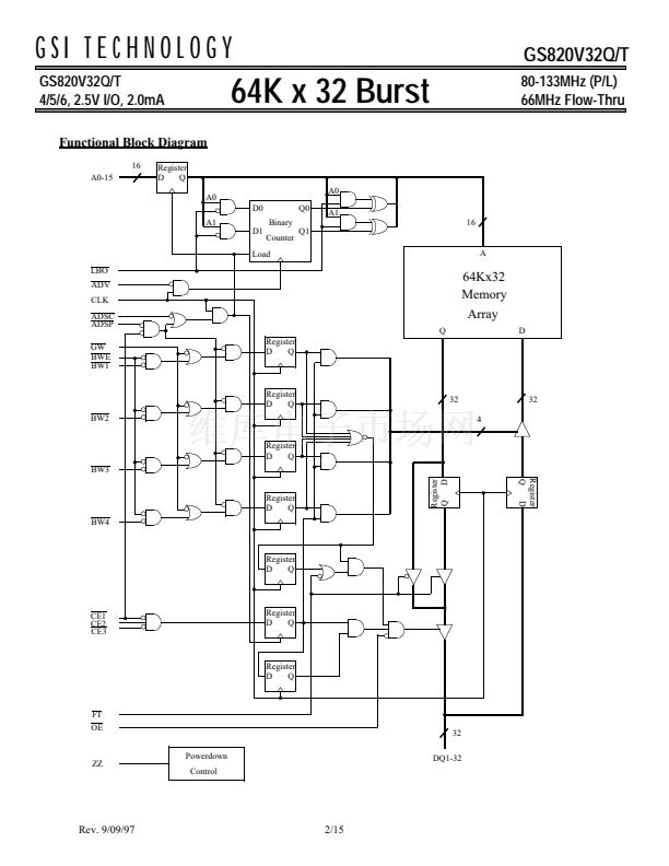
64K x 32 Burst
Functional Description
The GS820V32 is a 64Kx32 high performance synchronous SRAM
with 2 bit burst counter. It is designed to provide L2 Cache for Pen-
tium
TM
and other high performance CPU. Addresses (A0-15), data
IOs (DQ1-32), chip enables (CE1, CE2, CE3), address control inputs
(ADSP, ADSC, ADV) and write control inputs (BW1, BW2, BW3,
BW4, BWE, GW) are synchronous and are controlled by a positive
edge triggered clock (CLK).
Output enable (OE) and power down control (ZZ) are asynchro-
nous. 2 mode control pins (LBO & FT) define 4 operation modes
of linear/interleave burst order and output flow-thru/pipeline.
Burst can be initiated with either ADSP or ADSC inputs. Subse-
quent burst address are generated internally and are controlled by
ADV. The burst sequence is either interleave order (Pentium
TM
and X86) or linear order and is defined by LBO.
Output registers are provided and are controlled by FT mode pin.
With FT mode pin, Output registers can be programmed in either
pipeline mode for very high frequency operation (117MHz) or
flow-thru mode for reduced latency.
Byte write operation can be obtained through byte write enable
(BWE) input combined with 4 individual byte write signals
BW1-4. In addition, global write (GW) signal is also available to
write all bytes at once.
Low power state (standby mode) can be obtained either through
the assertion of ZZ signal or simply stop the clock (CLK). In
standby mode, memory data are still retained. Low power design
of 0.5mA standby are provided on L version.
The GS820V32 operates from a 3.3V power supply and all
inputs and outputs are LVTTL compatible. Separate output
power (VDDQ) and ground (VSSQ) pins are employed to de-
couple output noise from internal circuit and VDDQ allow user
the flexibility to employ lower output supply level like 2.5V.
GS820V32鈥檚 interface level is also compatble to 2.5V supply
level.
The GS820V32 is implemented with GSI鈥檚 high performance
CMOS technology and is available in JEDEC standard 100 lead
QFP ( Q version ) and TQFP ( T version) package.
Pin configuration
Top view
A6
A7
CE1
CE2
BW4
BW3
BW2
BW1
CE3
VDD
VSS
CLK
GW
BWE
OE
ADSC
ADSP
ADV
A8
A9
A0-15
CLK
BWE
BW1,BW2
BW3,BW4
GW
CE1,CE2, CE3
OE
ADV
ADSP, ADSC
DQ1-32
ZZ
FT
LBO
VDD
VSS
VDDQ
VSSQ
NC
Address Inputs
Clock Input
Byte Write Enable
Byte Write. BW1 for DQ1-8; BW2 for DQ9-16;
BW3 for DQ17-24; BW4 for DQ25-32
Global Write Enable
Chip Enable
Output Enable
Burst Address advance
Address Status
Data I/O
Power down control
Flow-Thru mode
Linear Burst mode
3.3V Power Supply
Ground
Output Power
(3.465Vmax)
Output Ground
No Connect
Supply,
2.375V
to
VDD
NC
DQ17
DQ18
VDDQ
VSSQ
DQ19
DQ20
DQ21
DQ22
VSSQ
VDDQ
DQ23
DQ24
FT
VDD
NC
VSS
DQ25
DQ26
VDDQ
VSSQ
DQ27
DQ28
DQ29
DQ30
VSSQ
VDDQ
DQ31
DQ32
NC
100 99 98 97 96 95 94 93 92 91 90 89 88 87 86 85 84 83 82 81
NC
80
1
DQ16
79
2
DQ15
78
3
VDDQ
77
4
VSSQ
76
5
DQ14
75
6
DQ13
74
7
DQ12
73
8
DQ11
72
9
71
10
VSSQ
70
11
VDDQ
69
12
DQ10
68
13
DQ9
67
14
VSS
66
15
NC
65
VDD
16
64
ZZ
17
63
DQ8
18
DQ7
62
19
61
20
VDDQ
60
21
VSSQ
59
22
DQ6
58
23
DQ5
57
24
DQ4
56
25
DQ3
55
VSSQ
26
54
VDDQ
27
53
DQ2
28
52
DQ1
29
51
NC
30
31 32 33 34 35 36 37 38 39 40 41 42 43 44 45 46 47 48 49 50
100 pin QFP / TQFP
Rev. 9/09/97
LBO
A4
A3
A2
A1
A0
NC
NC
VSS
VDD
NC
NC
A10
A11
A12
A13
A14
A15
NC
1/15


 1
1
 2
2
 3
3
 4
4
 5
5
 6
6
 7
7
 8
8
 9
9
 10
10
 11
11
 12
12
 13
13
 14
14
 15
15
