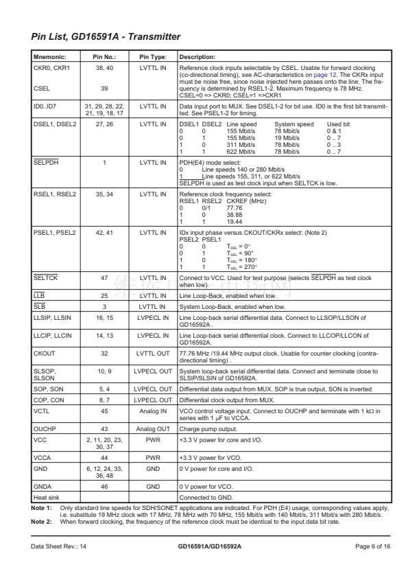
an Intel company
STM-4/STM-1/E4
3.3 V Multifunction
Transmitter and
Receiver
GD16591A/GD16592A
General Description
The GD16591A and GD16592A is a
front-end transmitter/receiver chip set de-
signed for multiple line interfaces:
u
STM-4 / OC-12
u
STM-1 / OC-3
u
PDH E4
This chip set is designed to interconnect
the high speed line interface to standard
CMOS ASICs providing low speed data
interface.
The GD16591A and GD16592A devices
are designed for use in both electrical
and optical line interface modules. The
devices support line speeds of:
u
140/155 Mbit/s NRZ mode for E4/
OC-3/STM-1 for an optical line inter-
face.
u
280/311 Mbit/s for E4/OC-3/STM-1 in
CMI mode for electrical line interface,
where en-/decoding is made at the
system site.
u
622 Mbit/s NRZ mode line speed for
OC-12/STM-4 operation.
The on-chip VCO and PLL blocks for
clock generation eliminate the need for
an external high-speed clock signal.
The GD16592A comprises a Limiting In-
put Amplifier (LIA), Clock & Data Recov-
ery, and a configurable DeMUX circuit.
The LIA offers a differential input sensi-
tivity of 10 mV peak to peak for the high-
speed serial input. A Lock Detect output
monitors the PLL locked onto the re-
ceived serial data.
The low-speed interface I/O麓s are
LVTTL-level, and the high-speed I/O麓s
are differential LVPECL levels (The LIA
input is usable as LVPECL input).
System (local) Loop-back and Line (re-
mote) Loop-back functions offer simpli-
fied manufacturing and field testing.
Low power consumption is achieved by
the 3.3 V single power supply and by
omitting all circuitry, which can easily be
implemented in the low speed system
ASIC, thus reducing the overall power
consumption.
The devices are housed in 48 pin
EDQUAD TQFP盲 plastic packages.
Features
General
l
Low jitter on-chip VCO and PLL.
Jitter performance exceeds the rec-
ommendations of ITU-T and Bellcore.
The chip set offers seven line and
system speed mode:
622 Mbit/s
蘆
78 Mbit/s, 8 bit
311 Mbit/s
蘆
78 Mbit/s, 4 bit
155 Mbit/s
蘆
78 Mbit/s, 2 bit
155 Mbit/s
蘆
19 Mbit/s, 8 bit
280 Mbit/s
蘆
70 Mbit/s, 4 bit
140 Mbit/s
蘆
70 Mbit/s, 2 bit
140 Mbit/s
蘆
17 Mbit/s, 8 bit
Four phase selectable clock to data
timing at parallel interface.
Selectable reference clock input fre-
quencies:
17.408/19.44MHz, 34.816/
38.88MHz, and 69.632/77.76MHz.
Loop Back for System & Line test
modes.
48 pin EDQUAD TQFP盲 packages.
Single supply: 3.1 ... 3.6 V.
l
l
l
l
l
l
l
CMOS System ASIC
Data
70/78 Mbit/s
17/19 Mbit/s
2 / 4 / 8 bit
Clock
GD16591A
MUX/
Retiming PLL
Line Interface
140/155 Mbit/s (optical)
280/311 Mbit/s (electrical)
622 Mbit/s (STM-4 opt.)
GD16591A (Transmitter)
l
8:1 / 4:1 / 2:1 MUX.
Differential transmitted clock output.
LVPECL data outputs.
Optional forward/counter clocking
scheme.
Power dissipation, typ.: 350 mW
l
l
l
System / Line Loop Back
l
Data
70/78 Mbit/s
17/19 Mbit/s
2 / 4 / 8 bit
Clock
Line Interface
140/155 Mbit/s (optical)
280/311 Mbit/s (electrical)
622 Mbit/s (STM-4 opt.)
GD16592A (Receiver)
l
GD16592A
DeMUX/
CDR with PLL
1:8 / 1:4 / 1:2 DeMUX.
Data Sheet Rev.: 14


 1
1
 2
2
 3
3
 4
4
 5
5
 6
6
 7
7
 8
8
 9
9
 10
10
 11
11
 12
12
 13
13
 14
14
 15
15
 16
16
