鈥?/div>
7.3A, 100V, R
DS(on)
= 0.35鈩?@V
GS
= 10 V
Low gate charge ( typical 5.8 nC)
Low Crss ( typical 10 pF)
Fast switching
100% avalanche tested
Improved dv/dt capability
175擄C maximum junction temperature rating
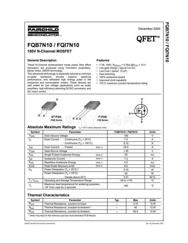
D
!
"
G
S
G
!
! "
"
"
D
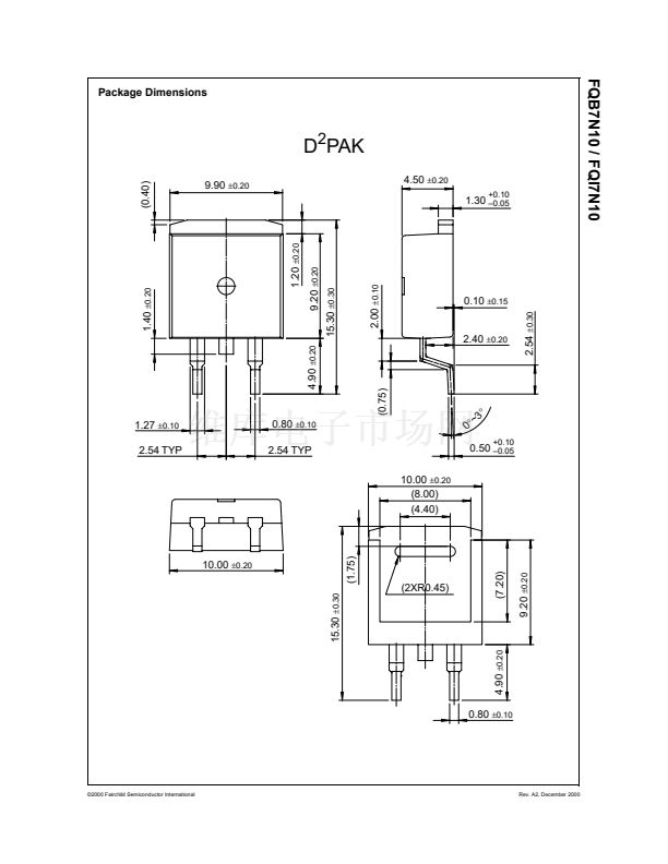
2
-PAK
FQB Series
G D S
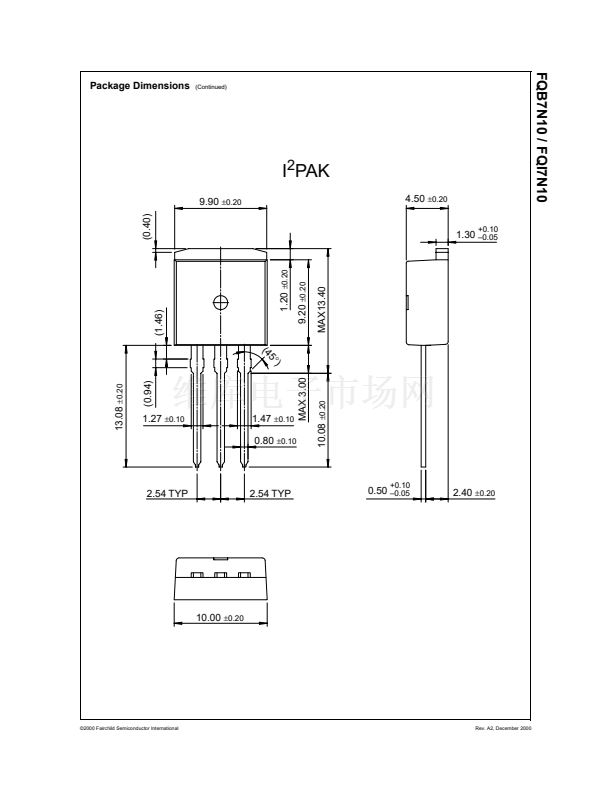
I
2
-PAK
FQI Series
!
S
Absolute Maximum Ratings
Symbol
V
DSS
I
D
I
DM
V
GSS
E
AS
I
AR
E
AR
dv/dt
P
D
T
C
= 25擄C unless otherwise noted
Parameter
Drain-Source Voltage
- Continuous (T
C
= 25擄C)
Drain Current
- Continuous (T
C
= 100擄C)
Drain Current
- Pulsed
(Note 1)
FQB7N10 / FQI7N10
100
7.3
5.15
29.2
鹵
25
(Note 2)
(Note 1)
(Note 1)
(Note 3)
Units
V
A
A
A
V
mJ
A
mJ
V/ns
W
W
W/擄C
擄C
擄C
Gate-Source Voltage
Single Pulsed Avalanche Energy
Avalanche Current
Repetitive Avalanche Energy
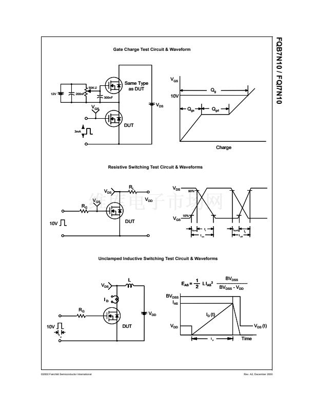
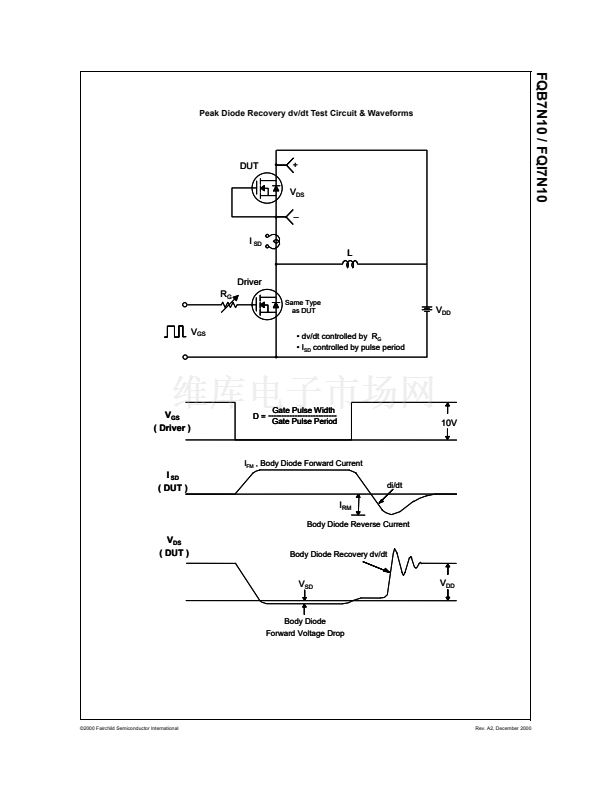
Peak Diode Recovery dv/dt
Power Dissipation (T
A
= 25擄C) *
Power Dissipation (T
C
= 25擄C)
50
7.3
4.0
6.0
3.75
40
0.27
-55 to +175
300
T
J
, T
STG
T
L
- Derate above 25擄C
Operating and Storage Temperature Range
Maximum lead temperature for soldering purposes,
1/8" from case for 5 seconds
Thermal Characteristics
Symbol
R
胃JC
R
胃JA
R
胃JA
Parameter
Thermal Resistance, Junction-to-Case
Thermal Resistance, Junction-to-Ambient *
Thermal Resistance, Junction-to-Ambient
Typ
--
--
--
Max
3.75
40
62.5
Units
擄C/W
擄C/W
擄C/W
* When mounted on the minimum pad size recommended (PCB Mount)
漏2000 Fairchild Semiconductor International
Rev. A2, December 2000


 1
1
 2
2
 3
3
 4
4
 5
5
 6
6
 7
7
 8
8
 9
9
