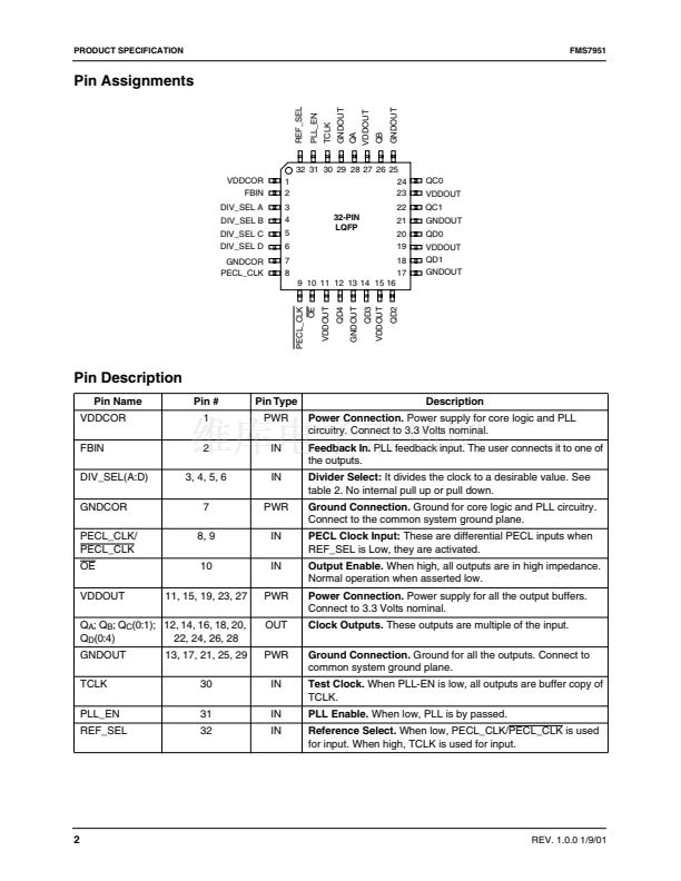
鈥?/div>
Low Voltage CMOS or PECL reference input
Up to 175 MHz of output frequency
Nine con鏗乬urable outputs
Output enable pin
250 pS of output to output skew
300 pS of Cycle to Cycle Jitter
V
DD
Range of 3.3V 鹵0.2V
Commercial temperature range
Available in 32 pin TQFP
It has four banks of con鏗乬urable outputs. By externally con-
necting one of the outputs to FBIN, the internal PLL will
lock in both phase and frequency to the incoming clock. Any
changes to the input clock will be tracked by the outputs.
Depending on the selected output for feedback connection,
the output frequencies will be as 1X, 2X or 4X of the input.
REF_SEL allows selection between PECL input or TCLK a
CMOS clock driven input. Connecting PLL_EN LOW and
REF_SEL HIGH will by pass the Phase locked loop. In this
mode, FMS7951 will be in clock buffer mode where any
clock applied to TCLK will be divided down to the four out-
put banks. This is ideal for system diagnostic test. When
PLL_EN is HIGH, the PLL is enabled, and any clock applied
to TCLK will be locked in both phase and frequency to
FBIN. PECL_CLK is activated when REF_SEL is high.
FMS7951 operates at 3.3 Volts and is available in 32 pin LQFP.
Description
FMS7951 is a high speed, zero delay, low skew clock driver. It
uses phase locked loop technology to generate frequencies up
to 175 MHz.
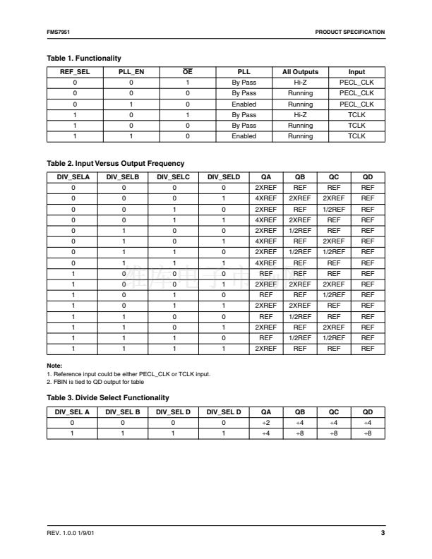
Block Diagram
REF_SEL
PLL_EN
OE
TCLK
QA
MUX
MUX
PECL_CLK
PECL_CLK
FBIN
QC1
QD0
QD1
DIV_SEL A
QD2
DIV_SEL B
DIV_SEL C
DIV_SEL D
QD4
Control
Logic
PLL
QC0
QB
QD3
REV. 1.0.0 1/9/01


 1
1
 2
2
 3
3
 4
4
 5
5
 6
6
 7
7
 8
8
