錚?/div>
) package. Read and
write operations are performed at the cross points of
the CK and the /CK. This high-speed data transfer is
realized by the 4 bits prefetch-pipelined architecture.
Data strobe (DQS and /DQS) both for read and write
are available for high speed and reliable data bus
design. By setting extended mode register, the on-chip
Delay Locked Loop (DLL) can be set enable or disable.
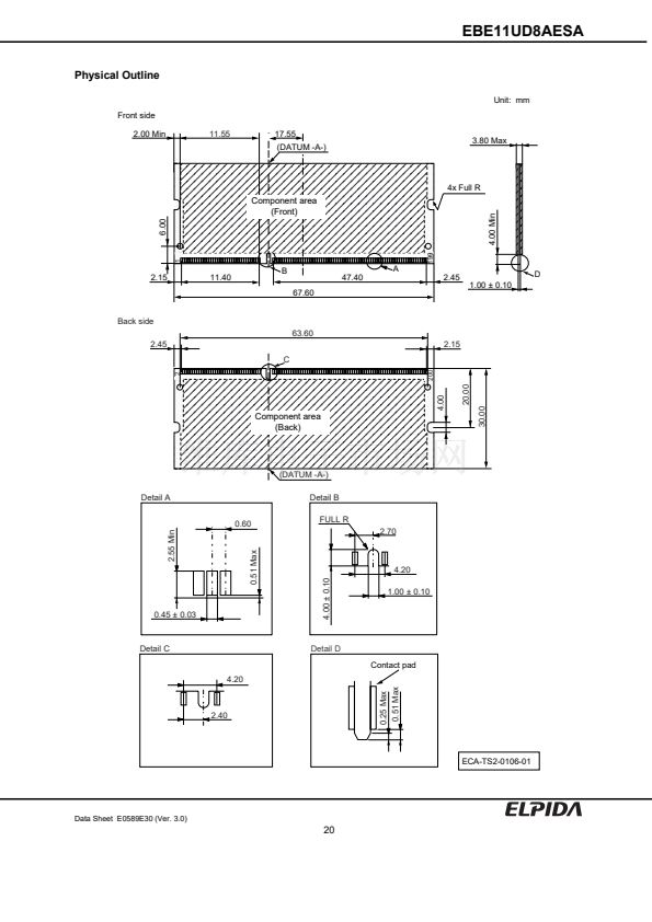
This module provides high density mounting without
utilizing surface mount technology.
Decoupling
capacitors are mounted beside each FBGA (碌BGA) on
the module board.
Note: Do not push the components or drop the
modules in order to avoid mechanical defects,
which may result in electrical defects.
Features
鈥?/div>
200-pin socket type small outline dual in line memory
module (SO-DIMM)
錚?/div>
PCB height: 30.0mm
錚?/div>
Lead pitch: 0.6mm
錚?/div>
Lead-free (RoHS compliant)
鈥?/div>
Power supply: VDD
=
1.8V
鹵
0.1V
鈥?/div>
Data rate: 667Mbps/533Mbps/400Mbps (max.)
鈥?/div>
SSTL_18 compatible I/O
鈥?/div>
Double-data-rate architecture: two data transfers per
clock cycle
鈥?/div>
Bi-directional, differential data strobe (DQS and
/DQS) is transmitted/received with data, to be used in
capturing data at the receiver
鈥?/div>
DQS is edge aligned with data for READs: center-
aligned with data for WRITEs
鈥?/div>
Differential clock inputs (CK and /CK)
鈥?/div>
DLL aligns DQ and DQS transitions with CK
transitions
鈥?/div>
Commands entered on each positive CK edge: data
and data mask referenced to both edges of DQS
鈥?/div>
Four internal banks for concurrent operation
(components)
鈥?/div>
Data mask (DM) for write data
鈥?/div>
Burst lengths: 4, 8
鈥?/div>
/CAS Latency (CL): 3, 4, 5
鈥?/div>
Auto precharge operation for each burst access
鈥?/div>
Auto refresh and self refresh modes
鈥?/div>
Average refresh period
錚?/div>
7.8碌s at 0擄C
鈮?/div>
TC
鈮?+85擄C
錚?/div>
3.9碌s at
+85擄C <
TC
鈮?+95擄C
鈥?/div>
Posted CAS by programmable additive latency for
better command and data bus efficiency
鈥?/div>
Off-Chip-Driver Impedance Adjustment and On-Die-
Termination for better signal quality
鈥?/div>
/DQS can be disabled for single-ended Data Strobe
operation
Document No. E0589E30 (Ver. 3.0)
Date Published July 2005 (K) Japan
Printed in Japan
URL: http://www.elpida.com
錚〦lpida
Memory, Inc. 2004-2005
EBE11UD8AESA-5C-E相關(guān)型號(hào)PDF文件下載
-
型號(hào)
版本
描述
廠商
下載
-
英文版
EURO BLOCKS TS & EB SERIES
ADAM-TECH
-
英文版
EURO BLOCKS TS & EB SERIES
ADAM-TECH [Adam...
-
英文版
EURO BLOCKS TS & EB SERIES
ADAM-TECH
-
英文版
EURO BLOCKS TS & EB SERIES
ADAM-TECH [Adam...
-
英文版
EURO BLOCKS TS & EB SERIES
ADAM-TECH
-
英文版
EURO BLOCKS TS & EB SERIES
ADAM-TECH [Adam...
-
英文版
EURO BLOCKS TS & EB SERIES
ADAM-TECH [Adam...
-
英文版
EURO BLOCKS TS & EB SERIES
ADAM-TECH
-
英文版
EURO BLOCKS TS & EB SERIES
ADAM-TECH [Adam...
-
英文版
EURO BLOCKS TS & EB SERIES
ADAM-TECH
-
英文版
1GB Registered DDR2 SDRAM DIMM
ELPIDA
-
英文版
1GB Registered DDR2 SDRAM DIMM
ELPIDA
-
英文版
1GB Registered DDR2 SDRAM DIMM
ELPIDA
-
英文版
1GB Unbuffered DDR2 SDRAM DIMM
ELPIDA
-
英文版
1GB Unbuffered DDR2 SDRAM DIMM
ELPIDA
-
英文版
1GB Registered DDR2 SDRAM DIMM (128M words x 72 bits, 1 Rank...
ELPIDA
-
英文版
1GB Registered DDR2 SDRAM DIMM (128M words x 72 bits, 1 Rank...
ELPIDA [El...
-
英文版
1GB Registered DDR2 SDRAM DIMM (128M words x 72 bits, 1 Rank...
ELPIDA
-
英文版
1GB Registered DDR2 SDRAM DIMM (128M words x 72 bits, 1 Rank...
ELPIDA [El...
-
英文版
1GB Registered DDR2 SDRAM DIMM (128M words x 72 bits, 1 Rank...
ELPIDA


 1
1
 2
2
 3
3
 4
4
 5
5
 6
6
 7
7
 8
8
 9
9
 10
10
 11
11
 12
12
 13
13
 14
14
 15
15
 16
16
 17
17
 18
18
 19
19
 20
20
 21
21
 22
22
