DS92CK16 3V BLVDS 1 to 6 Clock Buffer/Bus Transceiver
November 1999
DS92CK16
3V BLVDS 1 to 6 Clock Buffer/Bus Transceiver
General Description
The DS92CK16 1 to 6 Clock Buffer/Bus Transceiver is a one
to six CMOS differential clock distribution device utilizing Bus
Low Voltage Differential Signaling (BLVDS) technology. This
clock distribution device is designed for applications requir-
ing ultra low power dissipation, low noise, and high data
rates. The BLVDS side is a transceiver with a separate chan-
nel acting as a return/source clock.
The DS92CK16 accepts BLVDS (300 mV typical) differential
input levels, and translates them to 3V CMOS output levels.
An output enable pin OE , when high, forces all CLK
OUT
pins
high.
The device can be used a source synchronous driver. The
selection of the source driving is controlled by the CrdCLK
IN
and DE pins. This device can be the master clock, driving the
inputs of other clock I/O pins in a multipoint environment.
Easy master/slave clock selection is achieved along a back-
plane.
Features
Master/Slave clock selection in a backplane application
125 MHz operation (typical)
100 ps duty cycle distortion (typical)
50 ps channel to channel skew (typical)
3.3V power supply design
Glitch-free power on at CLKI/O pins
Low Power design (20 mA
@
3.3V static)
Accepts small swing (300 mV typical) differential signal
levels
n
Industrial temperature operating range (-40藲C to +85藲C)
n
Available in 24-pin TSSOP Packaging
n
n
n
n
n
n
n
n
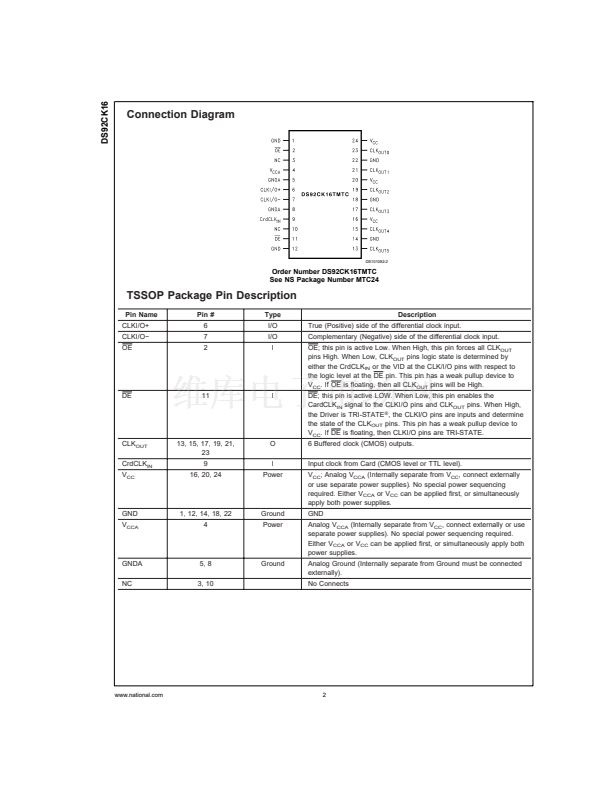
Function Diagram and Truth Table
DS101082-1
Receive Mode Truth Table
INPUT
OE
H
L
L
DE
H
H
H
CrdCLK
IN
X
X
X
(CLKI/O+)鈥?CLKI/O鈭?
X
VID鈮?0.07V
VID鈮?鈭?.07V
OUTPUT
CLK
OUT
H
H
L
Driver Mode Truth Table
INPUT
OE
L
L
H
H
H
DE
L
L
L
L
H
CrdCLK
IN
L
H
L
H
X
CLK/I/O+
L
H
L
H
Z
OUTPUT
CLKI/O鈭?/div>
H
L
H
L
Z
CLK
OUT
L
H
H
H
H
L = Low Logic State
H = High Logic State
X = Irrelevant
Z = TRI-STATE
TRI-STATE
廬
is a registered trademark of National Semiconductor Corporation.
漏 1999 National Semiconductor Corporation
DS101082
www.national.com


 1
1
 2
2
 3
3
 4
4
 5
5
 6
6
 7
7
 8
8
 9
9
 10
10
 11
11
